


除了电源时钟应该是fpga的第二重要的部分了,扮演着系统心脏的角色,是一切运算的基础。
使用HDL编程时往往就是以clk信号为驱动信号进行设计的,所以clk信号将直接影响整个芯片的逻辑。
学习清楚时钟的来龙去脉对软硬件的设计都是有好处的。
本文参考资料:
Cyclone II hand book
Altera时钟与PLL特性
http://www.altera.com/support/devices/pll_clock/pll-overview.html
Using PLLs in Cyclone Devices
http://www.altera.com/literature/hb/cyc/cyc_c51006.pdf
PLLs in Cyclone II Devices (PDF)
http://www.altera.com/literature/hb/cyc2/cyc2_cii51007.pdf
Clock Control Block (ALTCLKCTRL) Megafunction
http://www.altera.com/literature/ug/ug_altclock.pdf
先看下altera的描述(cyclone系列最多4个PLL 16条全局时钟网络)
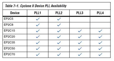
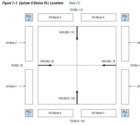
Cyclone II devices provide a global clock network and up to four phase-locked loops (PLLs).
The global clock network consists of up to 16 global clock lines that drive throughout the entire device.
The global clock network can provide clocks for all resources within the device, such as input/output elements (IOEs), LEs, embedded multipliers, and embedded memory blocks. The global clock lines can also be used for other high fan-out signals. Cyclon e II PLLs provide general-purpose clocking with clock synthesis and phase shifting as well @ external outputs for high-speed differential I/O support.
Flexible clock management circuitry
● Hierarchical clock network for up to 402.5-MHz performance
● Up to four PLLs per device provide clock multiplication and
division, phase shifting, programmable duty cycle, and external
clock outputs, allowing system-level clock management and
skew control
● Up to 16 global clock lines in the global clock network that drive
throughout the entire device
关于全局时钟
Each Altera® FPGA has an advanced, low-skew clock network. The number of clock networks and features offered varies depending on the device family (see Tables 1 and 2). The clock networks can be driven by CLK input pins, phase-locked loop (PLL) outputs, or internal logic, and can be used for other device-wide signals with large fan-outs, such as asynchronous clears and clock enables.
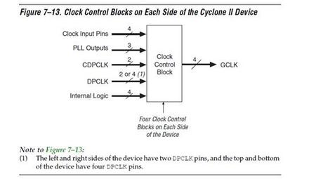
Each global clock network has a clock control block to select from a number of input clock sources (PLL clock outputs, CLK[] pins, DPCLK[] pins, and internal logic) to drive onto the global clock network. Ta b l e 2 – 2 lists how many PLLs, CLK[] pins, DPCLK[] pins, and global clock networks are available in each Cyclone II device. CLK[] pins are dedicated clock pins and DPCLK[] pins are dual-purpose clock pins.
The 16 or 8 global clock networks drive throughout the entire device. Dedicated clock pins (CLK[]), PLL outputs, the logic array, and dual-purpose clock (DPCLK[]) pins can also driv e the global clock
network.
The global clock network can provide clocks for all resources within the device, such as IOEs, LEs, memory blocks, and embedded multipliers. The global clock lines can also be used for control signals, such as clock enables and synchronous or asynchrono us clears fed from the external pin, or DQS signals for DDR SDRAM or QDRII SRAM interfaces. Internal logic can also drive the global clock network for internally generated global clocks and asynchronous clea rs, clock enables, or other control signals with large fan-out.
CYCLONE全局时钟与引脚


全局时钟引脚分为专用时钟引脚和两用时钟引脚
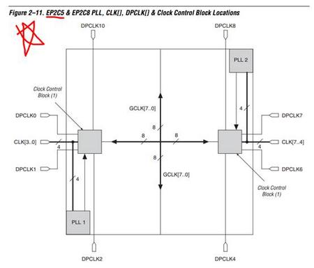
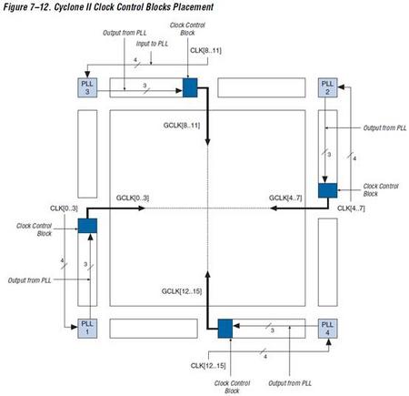
Larger Cyclone II devices (EP2C15 and larger devices) have 16 dedicated clock pins (CLK[15..0] , four pins on each side of the device). Smaller Cyclone II devices (EP2C5 and EP2C8 devices) have eight dedicated clock pins (CLK[7..0], four pins on left and right sides of the device). These
CLK pins drive the global clock network (GCLK), as shown in Figures 2–11 and 2–12.
Cyclone II devices have either 20 dual-purpose clock pins, DPCLK[19..0] or 8 dual-purpose clock pins, DPCLK[7..0]. In the larger Cyclone II devices (EP2C15 devices and higher), there are 20DPCLK pins; four on the left and right sides and six on the top and bottom of the device. The corner CDPCLK pins are first multiplexed before they drive into the clock control block. Since the signals pass through a multiplexer before feeding the clock control block, these signals incur
more delay to the clock control block than other DPCLK pins that directly feed the clock control block. In the smaller Cyclone II devices (EP2C5 and EP2C8 devices), there are eight DPCLK pins; two on each side of the device
These dual-purpose pins can connect to the global clock network for high-fanout control signals such as clocks, asynchronous clears, presets, and clock enables, or protocol control signals such as TRDY and IRDY for PCI, or DQS signals for external memory interfaces.

全局时钟的来源(时钟控制块)
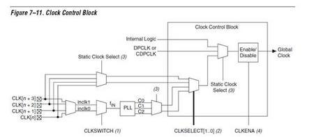
Notes to Figure 2–13:
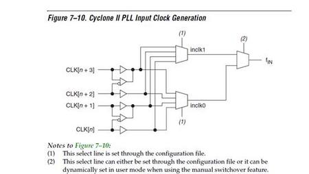
(1) The CLKSWITCH signal can either be set through the configuration file or it can be dynamically set when using the manual PLL switchover feature. The output of the multiplexer is the input reference clock (fIN) for the PLL.
(2) The CLKSELECT[1..0] signals are fed by internal logic and can be used to dynamically select the clock source for the global clock network when the device is in user mode.
(3) The static clock select signals are se t in the configuration file and cannot be dynamically controlled when the device is in user mode.
(4) Internal logic can be used to enabled or di sabled the global clock network in user mode.
Global Clock Network Distribution(全局时钟分布)
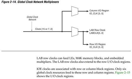
Cyclone II devices contains 16 global clock networks. The device uses multiplexers with these clocks to form six-bit buses to drive column IOE clocks, LAB row clocks, or row IOE clocks (see Figure 2–14). Another multiplexer at the LAB level selects two of the six LAB row clocks to feed
the LE registers within the LAB.
PLLs
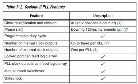
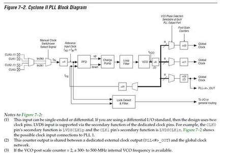
Cyclone II PLLs provide general-purpose clocking as well as support for
the following features:
■ Clock multiplication and division
■ Phase shifting
■ Programmable duty cycle
■ Up to three internal clock outputs
■ One dedicated external clock output
■ Clock outputs for differential I/O support
■ Manual clock switchover
■ Gated lock signal
■ Three different clock feedback modes
■ Control signals
Pins and Clock Network Connections
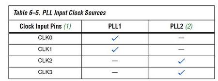
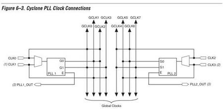
You must drive Cyclone PLLs by the dedicated clock input pins CLK[3..0]. Inverted clocks and internally generated clocks cannot drive the PLL. Table 6–5 shows which dedicated clock pin drives whichPLL input clock port.
PLL特性

Global Clock Network Power Down
The Cyclone II global clock network can be disabled (powered down) by
both static and dynamic approaches. When a clock network is powered
down, all the logic fed by the clock network is in an off-state, thereby
reducing the overall power consumption of the device.
The global clock networks that are not used are automatically powered
down through configuration bit settings in the configuration file
generated by the Quartus II software.
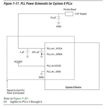
VCCA & GNDA
Each Cyclone II PLL uses separate VCC and ground pin pairs for their
analog circuitry. The analog circuit power and ground pin for each PLL is
called VCCA_PLL and GNDA_ PLL. Connect
the VCCA power pin to a 1.2-V power supply, even if you do not use the
PLL. Isolate the power connected to VCCA from the power to the rest of
the Cyclone II device or any other digital device on the board. You can use
one of three different methods of isolating the VCCA pin:
■ Use separate VCCA power planes
■ Use a partitioned VCCA island within the VCCINT plane
■ Use thick VCCA traces
Separate VCCA Power Plane
A mixed signal system is already partitioned into analog and digital
sections, each with its own power planes on the board. To isolate the VCCA
pin using a separate VCCA power plane, connect the VCCA pin to the
analog 1.2-V power plane.
Partitioned VCCA Island Within the VCCINT Plane
Fully digital systems do not have a separate analog power plane on the
board. Since it ' expensive to add new planes to the board, you can create
islands for VCCA_PLL. Figure 7–16 shows an example board layout with
an analog power island. The dielectric boundary that creates the island
should be 25 mils thick. Figure 7–16 shows a partitioned plane within
VCCINT for VCCA.
 /5
/5 
文章评论(0条评论)
登录后参与讨论