

当前绝大多数数字芯片都采用同步流水线设计。时钟频率是同步设计中的关键参数。因为一切功能都与时钟沿相关。这种设计的简化典型结构如下图所示:
前一级寄存器的输出经过组合逻辑运算后成为下一级寄存器的输入,一个复杂的设计会被分成很多级寄存器。为了保证数据可靠的向后级传递,每一级寄存器的建立保持时间必须满足。可以说,时序分析的本质就是分析寄存器的建立保持时间。
Currently, Nearly all of the digital ICs employ synchronous pipe-line structure. One of the most significant parameters is the clock frequency, because all of the functions related to clock edge. The typical structure can be simplified as Fig1.
The output of a source register participated in combinational logic, then act as destination register’s input. A complex design will be divided to many levels. Each level’s setup and hold time must be fulfilled. We can say, the essence of the timing analysis is the setup and hold time of each register.
There are three types of paths and two types of analysis run through our design. The three types of paths are clock paths, data path and Asynchronous path. The data path is easy to understand, it includes input/output of each register and the combinational logics. The clock path just like the clock wires in fig1. And the clear is one of the async path. The clock path and Asynchronous path is not as simple as we expected or at any case, even more difficult than data paths. The two types of analysis are Synchronous and Asynchronous. The Synchronous analysis focus on the relationship between clock and data path, and the Asynchronous on clock and async paths. Since the title is the basic concepts of timing analysis, the data path and related clock path is our main business.
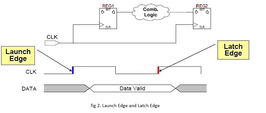
Concept 1. Launch Edge and Latch Edge

Launch Edge: the edge which “launches” the data from source register
Latch Edge: the edge which “latches” the data at destination register( with respect to the launch edge, selected by timing analyzer: typically 1 cycle)
When analyzing a path the TimeQuest analyzer determines the setup launch and latch edge times by finding the closest two active edges in the respective waveforms. When analyzing setup and hold relationships, the TimeQuest analyzer analyzes the path against two timing conditions for every possible setup relationship, not just the worst-case setup relationship; therefore, the
hold launch and latch times may be unrelated to the setup launch and latch edges.
Concept 2. Setup Time and Hold Time
Setup Time: the minimum time data signal must be stable BEFORE clock edge
Hold Time: the minimum time data signal must be stable AFTER clock edge
Concept3. Data Arrival Time
Data arrival time indicate the time when the data arrive at destination register’s D input.
Data Arrival Time = launch edge + Tclk1 + Tco + Tdata
Concept4. Clock Arrival Time
Clock arrival time indicate the time when the clock arrive at the destination register’s clock input.
Clock Arrival Time = latch edge + Tclk2
Concept5. Data Required Time
a. Data Required Time – Setup: The minimum time required for the data to get latched into the destination register
Data Required Time (setup) = Clock Arrival Time + Tsu
a. Data Required Time – Hold: The minimum time required for the data to get latched into the destination register
Data required Time (hold) = Clock Arrival Time + Th
Concept6. Setup Slack
Setup slack is the margin by which the setup timing requirement is met. It ensures launched data arrives in time to meet the latching requirement.
Setup Slack = Data Required Time – Data Arrival Time
Positive slack means Timing requirement met and Negative means not met.
Concept7. Hold Slack
Hold Slack is the margin by which the hold timing requirement is met. It ensures latch data is not corrupted by data from another launch edge.
Hold Slack = Data Arrival Time – Data Required Time
Same as the Setup Slack, Positive means Timing requirement met and Negative means not met.
 /2
/2 
用户1277994 2010-12-28 16:28