


其中8通道的每一通道都有一个低噪声放大器(LNA)、用于连续波(CW)多普勒模8×6差分交叉点开关、可变增益放大器(VGA)、抗混淆滤波器(AAF)和12 bit 模数转换器(ADC)。AD9271工作电压为1.8 V,以50 MSPS采样速率工作每通道功耗仅为150 mW。AD9271将8通道集成在一个16 mm × 16 mm,100引脚TQFP封装内,使超声诊断系统设计工程师增加通道数并增强图像质量,而无需加大设备的尺寸和功耗。
AD9271由于将许多高性能单元集成到单芯片内,所以能为急诊室、医生办公室和门诊所采用的便携式和车载超声系统提供优异的图像质量。AD9271的每一通道都具有30 dB可变增益范围,1.2 nV/√Hz@5 MHz折合到输入端噪声典型值、157 dB/√Hz, 输入动态范围、一个可编程三阶巴沃斯特(Butterworth)抗混淆滤波器、一个具有70 dB 信噪比(SNR)和80 dB无杂散动态范围(SFDR)的12 bit ADC。仅在显示模式下,可以关闭个别通道以延长电池寿命;或者在CW模式下当使用LNA时可以关闭ADC通道。
Octal LNA/VGA/AAF/ADC and Crosspoint Switch AD9271
The AD9271 is designed for low cost, low power, small size, and ease of use. It contains eight channels of a variable gain amp-lifier (VGA) with low noise preamplifier (LNA); an antialiasing filter (AAF); and a 12-bit, 10 MSPS to 50 MSPS analog-to-digital converter (ADC).
Each channel features a variable gain range of 30 dB, a fully differential signal path, an active input preamplifier termination, a maximum gain of up to 40 dB, and an ADC with a conversion rate of up to 50 MSPS. The channel is optimized for dynamic performance and low power in applications where a small package size is critical.
The LNA has a single-ended-to-differential gain that is selectable through the SPI. The LNA input noise is typically 1.2 nV/√Hz, and the combined input-referred noise of the entire channel is 1.4 nV/√Hz at maximum gain. Assuming a 15 MHz noise bandwidth (NBW) and a 15.6 dB LNA gain, the input SNR is roughly 86 dB. In CW Doppler mode, the LNA output drives a transconductance amp that is switched through an 8 × 6 differential crosspoint switch. The switch is programmable through the SPI.
主要特性:
8 channels of LNA, VGA, AAF, and ADC
Low noise preamplifier (LNA)
Input-referred noise = 1.2 nV/√Hz @ 7.5 MHz typical
SPI-programmable gain = 14 dB/15.6 dB/18 dB
Single-ended input; VIN maximum = 400 mV p-p/ 333 mV p-p/250 mV p-p
Dual-mode active input impedance matching
Bandwidth (BW) > 70 MHz
Full-scale (FS) output = 2 V p-p diff
Variable gain amplifier (VGA)
Gain range = −6 dB to +24 dB
Linear-in-dB gain control
Antialiasing filter (AAF)
3rd-order Butterworth cutoff
Programmable from 8 MHz to 18 MHz
Analog-to-digital converter (ADC)
12 bits at 10 MSPS to 50 MSPS
SNR = 70 dB
SFDR = 80 dB
Serial LVDS (ANSI-644, IEEE 1596.3 reduced range link)
Data and frame clock outputs
Includes crosspoint switch to support continuous wave (CW) Doppler
Low power, 150 mW/channel at 12 bits/40 MSPS (TGC)
90 mW/channel in CW Doppler
Single 1.8 V supply (3.3 V supply for CW Doppler output bias)
Flexible power-down modes
Overload recovery in <10 ns
Fast recovery from low power standby mode, <2 μs
100-pin TQFP
应用:
Medical imaging/ultrasound
Automotive radar
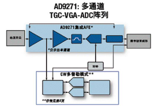
图1。应用方框图
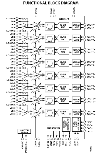
图2。方框图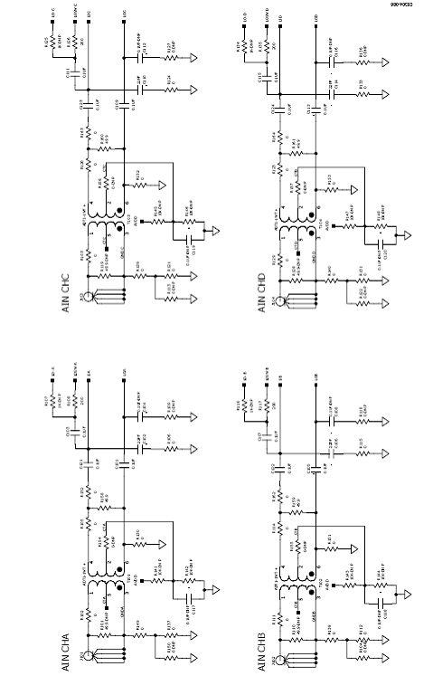
图3。评板电路图,DUT 模拟输入电路 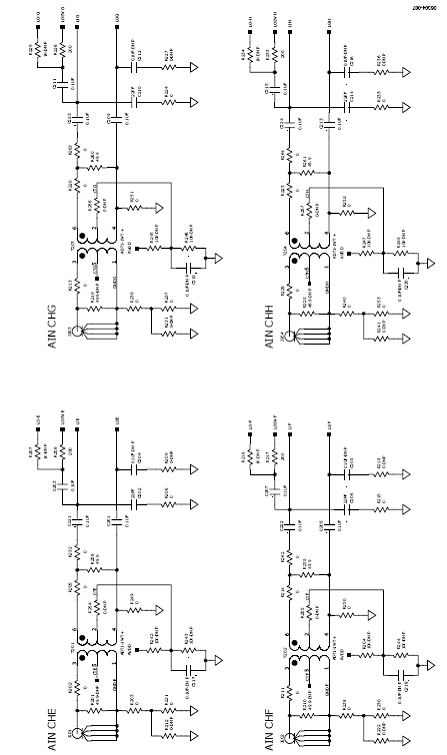
图3。评板电路图,DUT 模拟输入电路 (续)
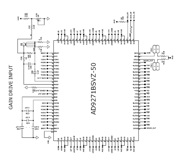
图4。评板电路图,DUT ,VREF和增益电路 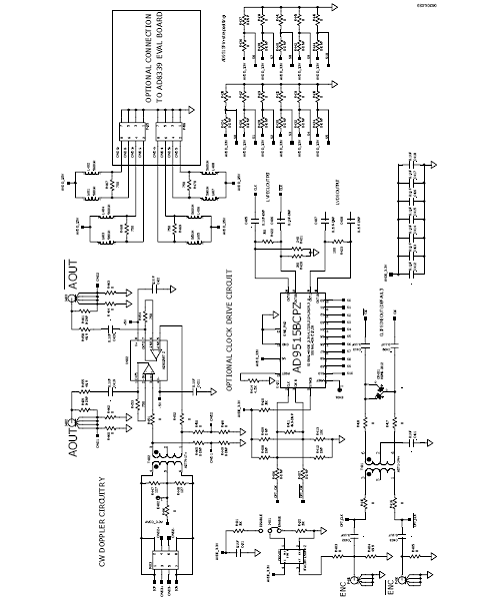
图5。评板电路图,时钟和CW Doppler电路
 /5
/5 
文章评论(0条评论)
登录后参与讨论