etail. Lots of it.
Store up to 500M samples at speeds as fast as 24MB/s.
Uncompromised Design
Logic is made of beautiful anodized aluminum.
Mini Size
Measuring in at 1.6"x1.6"x0.36," it goes with you anywhere.
The Best Wires
Logic comes with color-coded, non-kinking, ultra-flexible 22AWG 65/40 patch cable.
Protected Inputs
Logic has protection for ESD and overvoltage conditions built in.
Worry Free
If for any reason your Logic stops working we will replace or repair it for up to 1 year. If for some reason you want to return your Logic you can do so for up to 90 days.
Intuitive Viewport
To scroll the graph right and left, just click and drag. To zoom in or out, use your scroll wheel.
Extensive Metadata
Instantly see parameters like width, period, frequency and duty cycle. Hide parameters that are irrelevant for you.
m4-la Logic Analyzer for Xilinx ML403
m4-la is a Logic Analyzer written in VHDL for the Xilinx ML403 Development board featuring the Virtex4 FPGA. The user interface is written in C for Windows32 based platforms. Xilinx ISE and EDK tools compile the VHDL and MS Visual Studio compiles the UI.
Java Logic Analyzer Client
Beta
Java based logic analyzer client with pluggable protocol analyzers. It can be easily modified to use different analyzer hardware.
I got the sump.org Logic Analyzer running on a Xilinx Spartan-3E FPGA starter kit board. This wasn't too difficult, but there were some annoying problems that I'll share with you.
Installation and setup
Once again I downloaded and installed the 32-bit ISE WebPack 11.1 software on 32-bit Linux. It's a 2.8GB download which installs to roughly 5GB. (After deleting 1GB of .xinstall folders left from the installation.. wtf..) It seems that version 12.1 was released just recently and if you're using a version other than 11.1, or another operating system, then you may of course run into fewer problems, more problems, or just different problems.
Installation ran fine as a regular user. At the end of the installation I tried to do the upgrade to version 11.5 but didn't have enough disk space left. Now I can source the settings32.sh file in the directory I installed to and then run ise, impact, and the other programs.
I struggled for a while with iMPACT not finding the built-in Xilinx programmer cable on the starter kit board. There were two issues:
- Wrong firmware downloaded to the USB controller
- iMPACT stubbornly trying to use kernel windrvr instead of libusb
USB controller firmware
Xilinx provides a driver setup script which puts files in /etc/udev/rules.d and /usr/share but I prefered to make an ebuild for the Xilinx firmware package and have added it to my Portage overlay "stuge" which was included in the official layman list on 2010-06-14. If you're not using Gentoo you could most likely run the setup_pcusb script included in the tarball without issues, but note that newer versions of udevrequire some changes in the supplied rules.
iMPACT insists on ignoring libusb
Older versions of iMPACT used a really nasty kernel driver for accessing USB devices, but now it instead prefers to use libusb for the programmer access. Yay! But not so fast...
On my system iMPACT kept trying to use the old drivers, which I did not have installed and do not want to pollute my system with. According to Xilinx this means that "libusb is not installed", which is absolutely useless of course. It's very frustrating, and typical for closed source software, that information is not sufficiently specific. They need to document the actual assumptions made by their software, instead of publishing some nonsense high level description for what is a very low level system issue. Of course libusb was installed! Stupid.
Eventually I found the problem. It seems that iMPACT uses dlopen() to load "libusb.so", which is arguably a mistake by Xilinx developers. I believe that they should specify a filename with an explicit version instead, such as "libusb-0.1.so.4". The libusb-0.12-r5 package that I had installed unfortunately did not allow the unversioned dlopen() to work. The file found by dlopen("libusb.so") was /usr/lib/libusb.so, which was a small text file (a GNU ld script) used to redirect the linker to /lib/libusb.so when I compiled programs that used libusb. Similar files exist for other libraries. dlopen() needs a binary file however, it doesn't understand the linker script, so iMPACT was unable to load libusb, quietly resorted to requiring windrvr, and complained loudly when it wasn't found. There were no error messages about the failure to load libusb. I can't fix iMPACT, so I solved the problem by doing what I should have done long ago anyway; I removed libusb-0.1 and installed the libusb-compat-0.1.3 package instead, which provides backwards compatibility for libusb-0.1 applications and uses the much improved libusb-1.0 for communication. libusb-compat installs the binary library file in /usr/lib and /usr/lib/libusb.so is a symlink to it. Once it was installed iMPACT could find the programming cable via libusb without problems.
Downloading a logic analyzer
There's not much documentation for the sump.org logic analyzer package, which is too bad since it's a really useful design. There's even a minimal and pretty open hardware made explicitly for the sump.org design, and it costs only $45; the Open Logic Sniffer. If you have use for a LA and don't already have a suitable FPGA board around then I think the OLS is amazing value for money.
On the sump.org project page there are a few different versions available for download. The experimental Spartan 3E source is for the board that I used. The zip includes source for the PC Client (Java) and for the logic analyzer hardware design (VHDL). I added a sump-analyzer-0.8.1.ebuild to my overlay that builds the client and installs a launcher script called sump-analyzer. Non-Gentooers can download the slightly older v0.8 binary package to get a pre-built analyzer.jar, or compile their own with the following commands:
$ cd client/
$ javac -encoding iso-8859-1 $(find -name '*.java')
$ jar cfm analyzer.jar Manifest.txt $(find -name '*.class' -o -name '*.png')
Another great option is the highly portable sigrok open source software, which supports the sump hardware design as well as several other logic analyzer products.
From files to hardware
The fpga directory has the VHDL code that makes up the actual logic analyzer, and the UCF (User Constraint File) that specifies how the FPGA chip is connected. Now, let's make hardware from them:
Open ISE, create a new project, select Top-level source type HDL, click Next, set Family Spartan3E, Device XC3S500E, Package FG320, Speed -4 and Preferred Language VHDL, click Next twice (skip the "Create New Source" step), and in the "Add Existing Sources" step make sure to add all files in the fpga subdirectory except for la.ucf, la.vhd and license.txt, in particular la-S3ESK.ucf and la-S3ESK.vhd must be included. When you OK the "Project Summary" then ISE should add all 23 files without problems. Double click "Configure Target Device" under "Processes: la - Behavioral" in the lower half of the Design tab in the Design panel in ISE to run through Synthesis, Place & Route, and bitstream generation.
You may get a message about no iMPACT project file, just OK that so that iMPACT starts. Double-click "Boundary Scan" in the iMPACT Flows panel, then press Ctrl-I or select File->Initialize Chain in the menu. A dialog with settings for the three discovered devices appears, just OK that too. Double click the xc3s500e icon and assign the la.bit file created by ISE. Say No to the SPI or BPI PROM question. Right-click the xc3s500e icon and select Program. OK the same properties dialog again to send the bitstream to the FPGA.
When programming has succeeded the board is a logic analyzer, and you can start capturing signals! Don't forget a level shifter or series resistors if you want to capture 5V signals.
Notes
- SW1:0 sets baud rate: 00=115k2 01=57k6 10=38k4 11=19k2
- LED4:3 shows the baud rate set by SW1:0.
- LED1:0 shows the (active low) TX and RX signals.
- BTN_SOUTH is reset. LED6 shows the reset signal.
- LED7 shows the external clock signal. (DIP-8 socket)
- If capturing without an actual signal connected then remember to disable Noise Filter, or the logic analyzer doesn't see any data, and the capture seems to hang. Either apply an actual signal or close the capture, press BTN_SOUTH and then try again, making sure to disable the filter.
- iMPACT uses a SysV IPC semaphore to "lock" the download cable. If it isn't closed cleanly or if it crashes, it may start saying "Cable is LOCKED. Retrying..." in the log, which is of course wrong. Remove the semaphore with semget(0x240157b1,1,0),0,IPC_RMID,NULL) in a C program, or reboot, to get iMPACT to find the cable again.
- Look at la-S3ESK.ucf for the connections. All input channels are in the FX2 connector, but the first twelve are also on the more convenient J1, J2 and J4 headers.
FPGA-based Logic AnalyzerThis project was my entry in the Embedded Linux Journal's "Hack Embedded Linux for Fun and Prizes" contest. My goal was to create an inexpensive logic analyzer using an Altera FPGA and an embedded Linux processor from ZFLinux. Although I didn't win the contest, the logic analyzer works well and I am continuing to develop and support it just for fun.
Latest News...
| 12-31-04 | Please note that my email address has changed (see bottom of page). |
| 10-09-04 | Due to problems running the software under Windows XP, I have modified the code slightly and there is a new installation procedure. See Section 1.3 of the Help file for details. You can download the new version of logic2.exe (version 1.01) from the Software page. |
| 5-17-04 | I found a great site for anyone interested in FPGA design for fun projects, called FPGA4Fun. Check it out. |
| 9-18-03 | I have run out of blank PCBs, and I don't think that I will make any more. I sold about 15 of them, but no one has actually built a working board, as far as I know. I think that the soldering proved too difficult for most people. Also, the FPGA remains pretty expensive. I have started to port the design to one of the newer Cyclone FPGAs, which should be a lot cheaper, and might enable me to offer an assembled board for a reasonable price. I don't know when I'll get it done, though. |
| 9-2-2002 | Well, 6 months have gone by but I finally got around to building a new PP version prototype. I used a slower FPGA (the -3 speed, which is available from arrow.com), but the analyzer still seems to run fine at 100 MHz. With the slower chip, the trigger point is offset by one in the data display window, but everything else seems OK. I can't guarantee that everyone using the slower chip will get this performance, however, and the parts list still calls for the -1 part.
Now that the prototype is working, I am willing to supply blank PCBs to anyone who wants to build one. See below. |
| 3-3-2002 | I'm still working on getting a new FPGA, but I posted a picture of the PP board and the Gerber files on the PCB page. These should be considered preliminary until the board works. |
| 2-26-2002 | Arrgh! I assembled one of the new PP boards, and the FPGA seems to configure OK, but it doesn't work. I have tried some simple configuration files, just toggling pins, and nothing happens. I think that I have a bad FPGA. The one I used was on the shelf for a year. It'll take a few weeks to replace it. Sorry for the delay. |
| 1-29-2002 | I finished the PCB layout for the parallel port version, and sent in the Gerber files for PCB fab. Go to the PCB page to see the layout and parts list. |
| 1-21-2002 | I posted the schematic file for the parallel port version.
Go to the PCB page and look under "Schematics" to view or download. |
| 1-8-2002 | I posted the FPGA design files for the parallel port version.
Go to the FPGA page to download. |
| 12-23-2001 | I finally finished the application software!
Please go to the Software page download binaries, sources and documentation for logic2.exe. |
Networked Version
The contest prototype is shown below. It is a 32-channel logic analyzer based on an MZ104 processor board from Tri-M Systems, a network card, and a custom card which I designed, which I call the Analyzer PCB. The Analyzer PCB contains an FPGA, SRAM buffer, clock chip, clock switch, headers for data and clock inputs, an FPGA programming port and a PC/104 interface. The combination of the FPGA (which can be reconfigured under program control), and the MZ104 (which is essentially a complete PC running Linux), provides an exceptionally flexible instrument which can be adapted to many purposes besides logic analysis. In its current configuration it does not have a user interface, but is controlled by a remote Windows or Linux workstation over the network.

Parallel Port (PP) Version
Although the contest prototype used the ZFLinux embedded processor with an ethernet card, it is also possible to connect the Analyzer PCB directly to a host PC using the parallel port, without any other boards. This reduces the cost considerably, and is the best way to go if you just need a PC-based logic analyzer and don't want to develop a stand-alone instrument. You still have the option of using the board for lots of other purposes besides logic analysis, if you are willing to design your own logic with the Altera software.
I modified my prototype by adding an external PP interface board. Once I verified that it worked, I designed a new PCB which incorporates the PP interface. My first prototype didn't work, apparently due to a bad FPGA, so I built a second one, which is shown below. I used a lower speed grade FPGA than the original ( -3 instead of -1 ) which is much easier to get (you can usually get it online from arrow.com.) My prototype is working nicely at 100 MHz, but I don't guarantee that you will get the same performance. The parts list still calls for the -1 part.
Blank PCBs . . . Sorry, there are no more of these available ! ! !
USB Logic Analyzer
The goal of this project is to continue design for a USB logic analyzer to be used in the junior labartory. The design uses an Opal Kelly XEM3001 FPGA board which communicates over USB 2.0 to a GUI written in C#. more...
shom on 10.04.05 @ 03:50 PM CST [permalink]
Wednesday, April 26thProject Completion and Final Presentation
The USB Logic Analyzer is a fully functional standalone software application now. It is interfaced with the XEM3001 FPGA board and it reads simulated data (8-bit binary counter) from the FPGA over USB correctly. I was able to figure out how to communicate with the FPGA board and read the buffer and then use part of Jason's C++ program from last year to parse the data correctly. Since there is no external PC board (hardware part of the project was terminated when Jeff left the project) to sample signals the FPGA puts an 8-bit binary count value in the buffer, which is a great way to demonstrate functionality.
On the software side there have been tons of additions. I added in a data bus, I was able to read the logic lines and combine them into a hex value that is displayed on the plot surface. The user has the ability to select the lines added to the bus independent of the lines being plotted. The user can also save the plot in image format (png, jpeg, bmp, and gif) or in numeric format (csv). The saved CSV data file can be loaded back into the application in the future and all the software features can be used for analysis. The screen shot of the application visually explains a lot of these features.
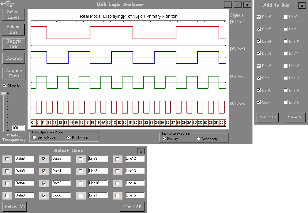
The project will be presented to faculty and students at the Senior Capstone Presentations on April 27th (tomorrow) at 8:30am. The presentation will be made available as part of the deliverables at later date. The final demonstration of the project will take place in Senior Lab on Friday, April 28th between 12 and 1 pm.
The final post to this website will be made once the final report has been approved for submission, at which point the project will be completed and all deliverables will be available here.
shom on 04.26.06 @ 01:52 PM CST [permalink]
Thursday, April 13thLive Demo @ the Bradley Student Expo
The project works!
The Opal Kelly XEM3001 sends an eight bit data stream over USB to the C# core program via some C++ executables (soon to converted to pure C#). The C# GUI plots the acquired data and still allows for all the functionality mentioned in previous entries!
Expo visitors will be able to play with the product using a 17" touch screen monitor (the GUI was modified for easier touch navigation).
The project is successful!
shom on 04.13.06 @ 03:56 AM CST [permalink] Kudos: -7 (+/-)
Thursday, March 30thGooeyer GUI
I have been adding a lot of GUI features. I modified the LineSelect form to include text boxes for all the lines so that an user can specify custom names. I added all the labels using the form designer and then manipulated their text, and position using code to reflect:
*what lines were selected
*what names they were given
*what line plot corresponds to that signal
Positioning was a difficult task especially with keeping resizing in mind.
I also improved error handling, especially focusing on application crashing when no lines were selected to be plotted. I found that this scenario was problematic for everything... plotting, resizing, refreshing, any form movement at all. Currently the GUI is fairly stable and mostly idiot proof.
My next challenge is to add the bus and use the mouse cursor to read the bus value and display it.
Here's a snapshot of the current GUI:
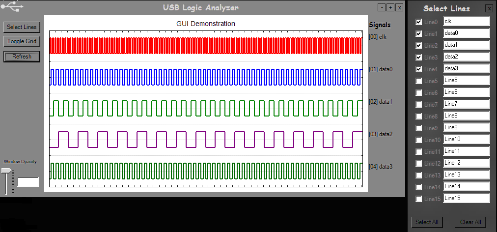
Again, if anyone is interested in helping me test the application, you can download and run the compiled binary (for Windows XP) and provide me with any feedback via e-mail.
shom on 03.30.06 @ 07:28 PM CST [permalink] Kudos: 4 (+/-)
Sunday, March 26thGooey GUI
I have mostly been working on and testing the GUI. Although, there is a separate time alloted for testing, the nature of GUI development leads to on spot testing. I will say that about 50% of the time I spend on the project is for development and the other 50% is testing. I have also changed how the data is stored internally form a double format to an integer format, this means less memory usage and faster processing. The logic level representation also had to be changed from the double representation:
'0.00' - Low
'0.50' - Indeterminate
'1.00' - High
to the integer representation:
'-1' - Low
'0' - Indeterminate
'1' - High
I have made a lot of progress on the GUI. The user now can:
*Select and plot only specific lines
*Lines can be selected in arbitary order
*Closing the main application closes all related windows
*Super impose a vertical grid, corresponding to the rising edge of the fastest signal
*Toggle the grid on and off
*Change the opacity of the application window
*Maximize/Minimize window
*Identify application by custom icon (in Windows ALT+TAB window)
Here's a snapshot of the current GUI.
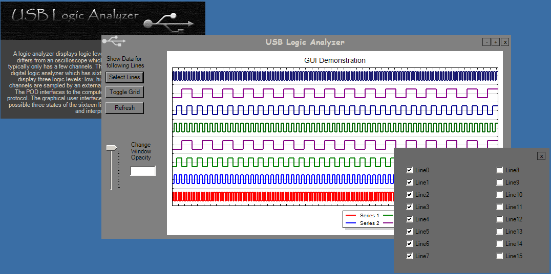
I am working on adding more features to the GUI and representing buses. If anyone is interested in helping me test the application, you can download and run the compiled binary (for Windows XP) and provide me with any feedback via e-mail.
shom on 03.26.06 @ 07:04 PM CST [permalink] Kudos: 6 (+/-)
Thursday, February 23rdGra Graph Graphics
The focus of the project has changed slightly due to the fact that Jeff Earlson is no longer working on the hardware. There is a possibility that there will be no board to test the USB data acquisition with. In light of these events I have decided to focus more detailed attention on to the graphics. The NPlot graphing library is very complicated because of its robustness, so adding a bus class has been a difficult task. more...
shom on 02.23.06 @ 04:58 PM CST [permalink] Kudos: 18 (+/-)
You’re not satisfied with the currently Logic Analyzer and would like to buy a brand new and low cost logic analyzer? OK, there is a great way here, where you can save your money and having a low cost logic analyzer here…
Yep, it’s time to develop a new PicLA logic analyzer, which it’s using an 18F2525 PIC microprocessor and a PC. In this project, the PIC is used as a hardware capture device, where it monitoring the data lines and records all the changes.

The analyzer can be operated in a “Fast Sampling” mode, which the data is being sampled into an internal 1K buffer on the PIC. There is another mode, the “Normal Sampling” or “Continuous Sampling” mode, which all the data changes are offloaded to the PC in real time.
This PicLA logic analyzer allows you to select the sampling in either 4 or 8 channels. Beside that, the 3584 or 7168 samples can be easily stored in “Fast Sampling” mode without any further modification. For the “Normal Sampling” there is no limit to the duration of the trace. The PC link will limit the “average” speed of the logic analyzer.
http://www.embedds.com/super-cool-mini-logic-analyzer/
probably want to build a prototype to test its operation. A common logic probe is more than enough, if the circuit is not complex; otherwise, you’ll require one or more complex driving signals to exercises its operation, then you need a more powerful testing tool here!
No matter you’re home hobbyists or experimenters, you might want to build the super cool Mini Logic Analyzer. This Mini Logic Analyzer is a simple and cheap logic analyzer, where it has up to 32 channels, 128Kb of memory for each channel, sampling rate up to 100 MHz, external clock input, external trigger input and much more.

The mini logic analyzer consists of a hardware, software and firmware interface. The interface will buffer the signals that are sent from the computer’s parallel port to the circuit to be tested. Beside that, it buffers the signals that are returned from the circuit to the computer and shifts their voltage levels, where it to make it compatible with the PC’s logic levels.
The analyzer incorporates two basic functional blocks, where as:
- A transistor buffer or inverter section; and
- An analog switch section that feeds voltage comparators.
This mini logic analyzer also has a LED tester, where it is a simple firmware created in order to test the functionality of mini logic analyzer hardware!
Most of you must have heard about logic analyzer before, but have you ever built a FPGA-based Logic Analyzer?
If you don’t know what the FPGA is, then you need to stick with us and read on the article. For your information, a field-programmable gate array (FPGA) is a semiconductor device that can be configured by the customer or designer after manufacturing, and that’s why it got the name “field-programmable.” To program an FPGA, you will need to specify how you want the chip to work with a logic circuit diagram or a source code in a hardware description language (HDL) first.

The FPGAs can be a very useful electronic component for implementing any logical function that an application-specific integrated circuit (ASIC) could perform. Furthermore, FPGAs contain programmable logic components called “logic blocks”, and a hierarchy of reconfigurable interconnects that allow the block to be wired together without any hassle at all. Logic block can be configured to perform complex combinational functions too!

Therefore, when you applied the FPGA into the logic analyzer, it would turn into a powerful tool that will benefit you in the end. What are you waiting for? Let get into the project and start the fun right now!
Ever since Steve Padnos let me borrow his commercial logic analyzer at CNC Workshop, I've been wishing I had one. Several years ago, fenn alerted me to minila, which consists of GPL hardware and software, but there don't seem to (presently) be any pre-built boards available for purchase, and I don't relish soldering surface-mount parts.
Then I stumbled on this FPGA Based Logic Analyzer. It's works on the still-available, $100 "S3BOARD", and the FPGA firmware is GPL. (It also has somewhat more memory than minila, and can also go up to 200MHz. On the other hand, it doesn't have a mode like minila's "state analysis", and it transfers over slow RS232 serial instead of EPP). I got the board today, and have some initial experiences to report.
I already had Xilinx Webpack installed from earlier work on mesa boards, so it wasn't hard to build the firmware, though it did confuse me for an hour how to program the so-called "platform flash" so that the board would boot in its logic analyzer personality. (the answer involves launching a program called "impact" to create the programming file for the flash, which is different from the programming file for the FPGA itself). Later on, I modified the constraints file to add internal pull-downs on the inputs; without that, the unused inputs worked as marvelous 120Hz antennas.
Later I had trouble getting the java-based GUI to work, because it could not find the serial communication library (and also wasn't compatible with gcj for some swing-related reason; I installed sun java instead). I ultimately found the answer, though I took the coward's way--copying files into the sun java installation area--instead of the method that alistair suggested one post further down. Like rscott13, I was just so relieved to have the software working at all.
Besides the start-up problems, I've hit one small bug in the GUI: I selected only channel-group 0 and 200MHz sample rate. What I got was my desired signal interleaved with "0"s. When I selected groups 0 and 1, 200MHz sample rate worked. (so far any input signals I've tried have been at much more modest rates of under 5MHz)
The FPGA is not 5V tolerant and no protection is built into the board. The FPGA input pins do have protection diodes, though, so I designed a separate "input conditioning" board which simply consists of a 1.4K series resistor on each input signal. It also breaks the signals into the 4 groups of 8 and provides a ground for each group. This might allow something like .35mA of protection diode current per input, while the datasheet permits up to 100mA per input on up to 100 inputs (which I imagine has to be a mistake, or at least subject to other thermal limits). This simple method for 5V compatability seems to work so far.
When capturing traces of modest length (8k samples), the delay imposed by the serial link is tolerable. When getting a full 256k samples, though, you're looking more than a moment of time. My next modification may be to place a 1MB/s serial output on some unused pins--maybe the PS/2 connector--and run those through the USB-serial chip on an arduino board, which is supposed to work with rates up to 3Mb/s. (1MB/s is the fastest rate that is exactly obtainable by both devices) If that works i'll buy a dedicated TTL-serial-to-USB converter for the board.
http://www.gadgetfactory.net/gf/project/butterflylogic/ http://dangerousprototypes.com/open-logic-sniffer http://www.seeedstudio.com/depot/open-workbench-logic-sniffer-p-612.html?cPath=61_68 It is an FPGA-based 16-channel logic analyzer that works with the SUMP open-source logic analyzer client software: http://www.sump.org/projects/analyzer/ http://oakmicros.com/content/downloads/View-document/Logic-Analyzer-User-Guide.html http://dangerousprototypes.com/2010/05/31/windows-logic-sniffer-client-update/ |
|
Logic Analyzer Adapter for Xilinx boards
http://www.kdvelectronics.eu/probe_adapter/probe_adapter.html
Logic Analyzer Adapter for Xilinx boards
Description
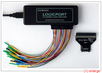
The Intronix Logicport is a small USB-based logic analyzer. It has 34 channels, two of which can be used as clock inputs, and does state analysis at 200 MHz. Sample depth without compression is 2048 samples per channel. While the Logicport is modest in specifications, for many tasks it may well be all you need. I mainly use the Logicport for Xilinx FPGA projects.
The Logicport connects to the system under test using one of three ways:
- The Logicport comes standard with a 38-wire flying lead probe. These are 38 individual color-coded wires - 34 signal and 4 ground wires - which you connect one by one.
- A 38-pin Mictor ("Matched Impedance Connector") adapter is also available.
- The Logicport uses a standard 40-pin IDC connector, so you may be able to use a 40-wire IDE hard drive cable as test lead if clock frequencies are low enough and your cable short enough. If you use an IDE hard drive cable as test lead, make sure the IDE cable is a full 40-wire cable, and not one with pin 20 disabled.
Logicport logic analyzer with flying leads. To the right, the Mictor adapter.
Problem
Plugging 38 color-coded leads on 38 header pins on my Xilinx Development Board is time-consuming and error-prone.
Solution
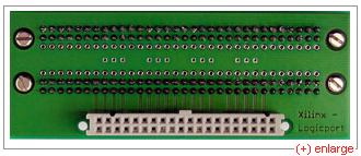
Instead of connecting through a flying lead probe, connect through a custom adapter.
Benefits:
- The adapter simply plugs into the target system. No flying leads.
- The Logicport plugs into the adapter. No cables.
Xilinx to Logicport adapter| Adapter, front view. | Adapter, back view. |
|---|
 |
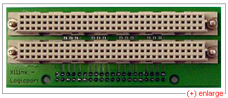 |
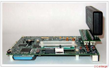
Adapter sitting on a Xilinx ML403, using the Xilinx Generic Interface (XGI) connector. Other Xilinx developments boards feature the same connector. Please note the XGI connector is non-polarized. Make sure you do not plug in the adapter upside-down. Plugging in the adapter upside-down will short some FPGA outputs to ground, possibly damaging them.
ML403 board, with logic analyzer sitting on adapter.
This setup allows you to look at 32 signals, a clock enable and a clock inside the FPGA in real time at reasonable cost.
Ground loops
When connecting the Logicport to a circuit, you are connecting the circuit ground to the PC ground through the USB cable. If circuit ground and PC ground have a different potential, connecting them produces a ground loop. This is a general problem, which may also occur in USB oscilloscopes, for instance.
A simple solution against ground loops, sufficient for occasional use, is using a notebook with the AC cord unplugged, running off the battery. My personal choice has been to put a 100VA isolation transformer Block TIM-100 between notebook and mains and forgetting all about ground loops. Connecting the notebook to the network using unshielded twisted pair ethernet does not break the isolation.
Availability
I neither manufacture nor sell these adapters. If you want one, you will have to make one yourself. If you wish to have the printed circuit board made for you, download the archive for the adapter and extract all files. Send the .brd file to a PCB house such as pcb-pool. The .brd file is anEagle format file. Ask for a double-sided PCB with solder mask, no silkscreen, no electrical testing.
Downloads
The schematics and board layout can be downloaded:
You can use the sample ISE project as a simple electrical test. You should get the following waveform:
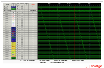
Ring counter output.
Last update page: October 9, 2007
34 CHANNEL LA1034 LOGICPORT LOGIC ANALYZER
http://www.pctestinstruments.com/index.htm
http://opencores.org/project,openverifla
openVeriFLA - FPGA logic analyzer :: Overview
Details
Name: openverifla
Created: Jul 31, 2007
Updated: Mar 3, 2008
SVN Updated: No data
SVN: Browse
Latest version: download
Statistics: View
Other project properties
Category: Library
Language: Verilog
Development status: Stable
Additional info: FPGA proven
WishBone Compliant: No
License: GPL
openVeriFLA - FPGA logic analyzer
openVeriFLA is an FPGA integrated logic analyzer.
It can be used for in-circuit debugging and verification
of the FPGA based applications.
The FPGA part is written in verilog. The PC part
is written in java and is platform independent.
Being simple and well documented, the openVeriFLA library
is well suited for didactical purposes and academic use.
For more information, please unzip the project archive
and read the reference manual.
Features
- on-the-fly capture, graphical display, testing automation
IMAGE: verifla_keyboard_protocol_verification_50procent.jpg
FILE: verifla_keyboard_protocol_verification_50procent.jpg
DESCRIPTION: The FPGA capture of a keyboard controller signals
http://lekernel.net/blog/?p=72
USB Logic Analyzer
I designed and built this board in mid 2007 as my very first FPGA (and soldering-intensive for that time) project. Its purpose was to sample a reasonable number of logic channels (24) at a high rate, and stream the data to a computer through high-speed USB 2.0. But as the board is FPGA-based, it can be used for any application requiring a high transfer rate (hundreds of MBit/s) with a computer.
The project has gained some popularity from DIY sites, but be sure to check out the “Erratum” section below. Feel free to contribute fixed PCB files and proper software and FPGA design.
Photo and screenshot

(Thanks PCB-POOL for providing the circuit board)

Description
The board uses a small Altera Cyclone II FPGA (EP2C5T144C7N) and a NET2272 USB controller from NetChip(this part is a bit hard to find, I got mine from Mouser Electronics). The FPGA was programmed with a mix of VHDL and schematic diagrams, and includes a minimal USB protocol handler entirely in hardware (no softcore processor was used).
The board can be self- or USB- powered. The 5V from USB is converted to 3.3V (used by the NET2272 and FPGA I/O) by a LTC3411 switching regulator and to 1.2V by another LTC3411 regulator (used by the FPGA core). The 3.3V supply is also converted to 2.5V by a linear regulator, and used to supply parts of the NET2272.
The board is equipped with three connectors :
- one 10-pin connector on top of the board is for JTAG configuration of the FPGA. Its pinout is the same as on Altera development boards, so you can directly use Altera Byteblaster cables for instance.
- one 10-pin connector on the bottom is for connecting a serial FPGA configuration device
- one 26-pin connector on the bottom is for connecting the probes (or whatever device you fancy

Erratum
- The software and the FPGA code are badly designed
- The switching regulators need additional 100nF decoupling capacitors close to their input pins, or they can go unstable. IN EVERY CASE, DOUBLE-CHECK POWER SUPPLY VOLTAGES BEFORE SOLDERING THE FPGA AND THE NET2272 !
- The wiring of the USB plug is incorrect, pin 5 is GND (not shield) and pin 4 can be left unconnected.
- Bit 16 of the NET2272 bus is not connected to the FPGA (the NET2272 can operate in 8-bit mode anyway, but it’s slower).
SMD soldering
Some people think that soldering small SMD parts such as TQFPs require lots of equipment. The board depicted above was entirely soldered by hand using an off-the-shelf soldering iron and a bit of inexpensive solder wick. A TQFP-144 can be soldered in about 10 minutes with very little equipment !
- For SMD parts with a low pin count (ie. resistors, capacitors, small SOICs…) first make a solder ball on one of the PCB pads. Then heat it with the iron while plunging one pin of the part in the melted solder ball, with a pair of tweezers. Remove the soldering iron. You don’t care if the solder is not good, its only purpose is to prevent the part from moving. Then, solder the other end of the component (be careful not to heat too much, not only you may damage the component but also you risk melting the first solder holding it), and rework the first solder.
Dont’t mess around with SMD glue, it’s a complete waste of time and money compared to this technique.
- For SMD parts with a lot of small pins (ie. TQFPs, uMAXs, …) you would go mad trying to solder each pin individually while avoiding short-circuits (and not heating the part too much !). First, prevent the part from moving using approximately the same technique as before : place the part very precisely using your hand or a pair of tweezers, then make a drop of solder on a couple of neighbouring pins (you don’t care if you short them). Double check all pins are correctly placed on their corresponding PCB pads – it will be very difficult to correct an error afterwards. If they are not, melt the solder and carefully move the part. Once the part is correctly placed, make solder bumps on all pins, shorting them all together. Then, using solder wick, remove the excess solder which should go away easily, leaving just enough solder on each pin. Remove the solder residues this method leaves all around (nail polish dissolvent and a toothbrush work as good as flux cleaners, and is a lot cheaper. But get one without acetone, as it can damage some plastics). Visually inspect the connections (if they are short circuits, it is often easier to add a lot of solder over the shorted pins then to remove it using the wick)
Downloads
Schematics (PDF)
PCB layout (PDF)
Altium Designer files
Sample driver
Sample FPGA design
http://www.sump.org/projects/analyzer/
FPGA Based Logic Analyzer
The outcome of this project is a logic analysator for home use.
The project includes the actual analyzer in VHDL (for Spartan 3 FPGA) and a PC Software for the end user. The design employs a FPGA board that can be obtained easily.
Features
- 16 channels at 200MHz sampling rate
- 32 channels up to 100MHz sampling rate
- state analysis up to 50MHz using external clock
- 256KSamples memory
- noise filter
- complex serial and parallel trigger with four stages
- externally available sampling clock to drive add-ons (like ADCs)
- connects via EIA232/RS232 (works with usb to serial adapters)
- Java based viewing software (see PC Client for details)
- I2C & SPI protocol analysis
Hardware
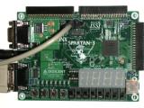
The device uses a Xilinx Spartan 3 Starter Kit (DO-SPAR3-DK) evaluation board manufactured by Digilent. It features a XC3S200-4 FPGA with 4ns propagation delay and 3840 cells. Onboard are 1MByte of 10ns SRAM and plenty connectors that can be used as signal inputs.
To construct a comparable board from scratch would be a tough task for a home project. Especially the really low price of about USD100 makes it pointless to try to compete with this "mass product". All that remains to be done is to program the FPGA. For an overview of the VHDL code see:
FPGA VHDL Model
To learn how to communicate with the analyzer read:
Communications Protocol
Client
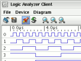
A java client is used to access the device from almost any PC with a serial port. The client uses the RXTX library for serial port communications which is available for 34 platforms including Linux, Windows and Solaris.
It has been developed with jdk 1.4.2 but might work with older versions. More information about the client can be found on its page:
Logic Analyzer Client
License
Files found in the downloadable archives below are released under the GNU GPL.
Downloads
Packages contain all that is needed for PC client, FPGA and tester.
See history for a list of changes between versions
"Official" Version
Logic Analyzer Package v0.8 - Binary (2007-03-03)
Logic Analyzer Package v0.8 - Source (2007-03-03)
User Contributed Versions
These downloads are provided without any testing.
Altera DE2: Experimental Port to Verilog for Altera DE2 Board - Source (2007-05-21)
(Contributed by Kenneth Tsang. Uses external SRAM.)
Altera DE2: Experimental Port to Verilog for Altera DE2 Board - Source (2007-05-21)
(Contributed by Kenneth Tsang. Uses internal M4K SRAM.)
Spartan 3E: Experimental Version for New Spartan 3E Starter Kit - Source (2007-03-08)
(Contributed by Jonas Diemer. Uses internal BRAM with optional RLE.)
Archive
Logic Analyzer Package v0.7 - Source (2006-12-31)
Logic Analyzer Package v0.6 - Source (2006-08-19)
Logic Analyzer Package v0.5 - Source (2006-06-18)
Logic Analyzer Package v0.4 - Source (2006-05-23)
Logic Analyzer Package v0.3 - Source (2006-05-05)
http://gadgetforge.gadgetfactory.net/gf/project/lax/
The "Sump" Logic Analyzer supports 32 channels with 4K sample memory up to 100MHz. The included Java client application allows waveform exploration as well as SPI and I2C protocol analysis. The project is optimized to run on the Butterfly Platform hardware.
Features
- 4K sample memory (expandable in future designs)
- 32 channels sampling at 100MHz
- 16 channels sampling at 200MHz (experimental)
- Four stage serial and parallel triggering
- External clock input
- Noise filter
- RLE built into the hardware to make the most of available memory.
- SPI protocol analysis (SPI debugger)
- I2C protocol analysis (I2C debugger)
- UART protocol analysis (UART debugger)
- State Analysis
Additional Benefits
- Completely Open Source hardware and software with development communities working on new functionality.
- Since the Logic Analyzer is built on very flexible FPGA technology it is not limited to being a Logic Analyzer. Future projects that will be supported by the same "Butterfly Light" hardware include:
- Flash Programmer
- Oscilloscope
- Variable Power Supply
- The same Butterfly Hardware can be used as a FPGA development platform supported by an Open Source community actively developing projects such as:
- 8 bit microcontrollers
- Hardware Modules to implement additional functionality such as more memory and input buffers.
- 32 bit RISC processors that can run ucLinux
- Java Virtual Machines to support Java development.
Limitations
- The FPGA can only sample 1.2V, 2.5V, and 3.3V. Any higher voltages can damage the input pins of the FPGA. Given time a plugin board will be developed to address this issue.
- Operation above 100MHz is not well tested.
http://www.usbee.com/suite.html
Easy to use Logic Analyzer / Oscilloscope
The USBee Suite is powerful electronic signal analysis software for your USBee Test Pod. It starts out as an easy to use Logic Analyzer and Oscilloscope and adds serial bus decoding and world class configurability that lets you solve your electronic problems quickly! Some of the serial busses that are decoded include: I2C, SPI, Async, USB, CAN, 1-Wire, PS/2, SMBus, I2S, Sync Serial and even your own Custom Busses.
World-Class User Interface
You look at a Logic Analyzer / Oscilloscope for extended lengths of time. Why don't you make sure you can enjoy it at the same time? The USBee Suite software lets you choose the look and feel of the interface and saves that information for when you come back to it again.
Best of all the USBee Suite Standard is Free! |  |
The USBee Suite Standard is a free download and will run in Demo mode without a USBee, or on any USBee SX, USBee ZX, USBee AX-Standard, USBee AX-Plus, USBee AX-Pro, USBee DX or BusBee Test Pod. So take it for a spin. If it has been a while since you've used your USBee, pull it out of your pocket and experience the power of the USBee Suite.
Upgrade to the USBee Suite Pro for State-of-the-Art Debugging Features!
The USBee Suite Pro builds upon the rich features set of the Standard version and adds high powered capabilities such as Complex Event Searching, PacketPresenter custom packet decoder, Smart Markers, enhanced PacketPresenter API for developers, annotation capabilites, enhanced acquisition control for repeated measurements, display control, analog channel scaling, analog bus decoding, and enhanced file importing and exporting. |








 /3
/3 

文章评论(0条评论)
登录后参与讨论