

The CAD library is the starting point that affects every process from PCB layout through PCB manufacturing and assembly. There are dozens of things to consider when creating a CAD library. Each can directly affect the quality of the part placement, via fanout, trace routing, post processing, fabrication and assembly processes. Yet, they are often overlooked.
This paper, the first in a series dedicated to CAD library quality, describes each aspect you should consider when creating Molded Body Component library parts. It also describes the impact each feature has in the PCB process.
There are three types of CAD library parts; plated through hole (PTH), surface mount devices (SMD), and a combination of the two technologies. SMD and PTH CAD libraries are distinctively different but the same basic rules apply to both technologies: “snap” and “round-off” CAD library land (pad) shapes to 0.05 mm increments. All of the component land patterns represented in this document are included in the xDX Land Pattern Creator that comes free with every seat of PADS® PCB designsoftware.
Today, 90% of all component manufacturers list their component package dimensions in metric units. For example, Texas Instruments only provides metric units for their component packages. TI is following the metric mandate by all world standards organizations and 99% of all world governments. Accordingly, this paper utilizes metric units for CAD library development.
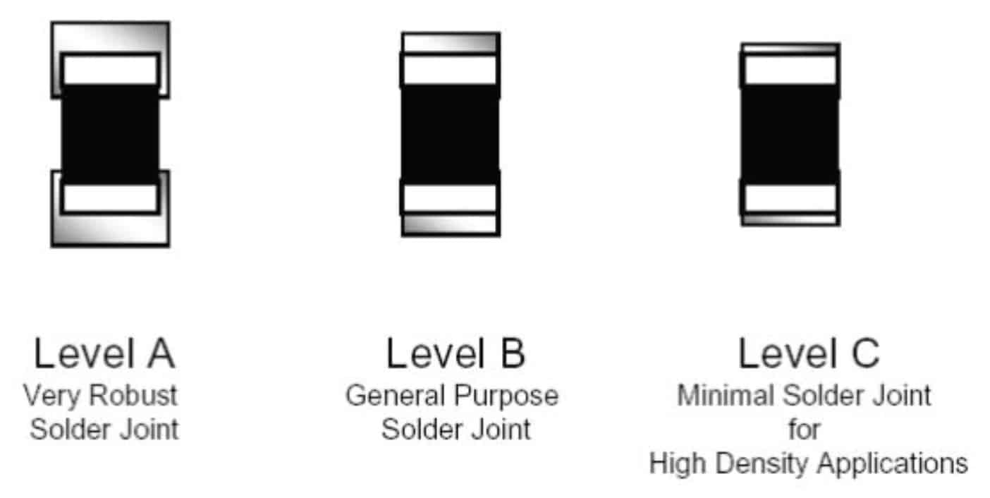
The examples in this document are calculated utilizing the nominal environment as defined in IPC-7351B’s standard 3-tier CAD library system: See Figure 1.
1. Level A = Most – for military and medical applications.
2. Level B = Nominal – for controlled environment desktop.
3. Level C = Least – for cell phones and hand-held devices.

With the exception of chip components, the next most-popular component family on a PCB designlayout is the molded body tantalum capacitor (CAPM). The CAPM components have an “L-Bend” component lead form. Most molded body tantalum capacitors are metric by default, including their standard EIA names:
The common component families that use the molded body package are:
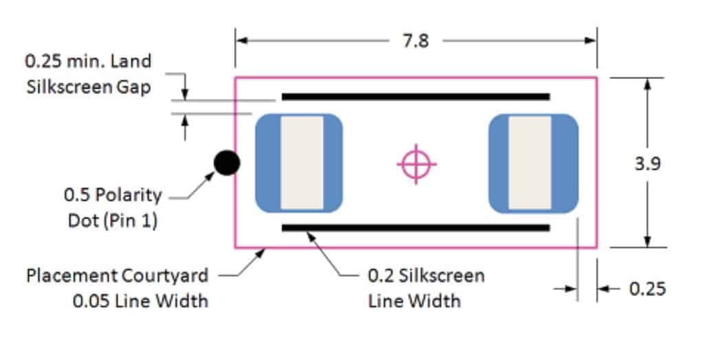
Figure 2 provides the 6032 component and land pattern dimensions. A rule was broken to create this land pattern. Instead of a 1.0 mm land placement round-off, a 2.0 mm land placement round-off was used to snap the land centers on a 0.5 mm grid from the center of the land pattern. When the land pattern is placed on a 0.5 mm grid, the land centers fall on a 0.5 mm grid. This improves the via fanout seen in Figure 4.

Figure 3 illustrates the silkscreen and placement courtyard rules and sizes. The illustration shows the component leads on top of the lands for graphic representation.

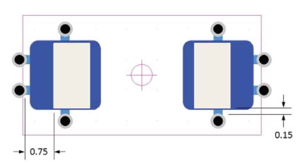
Figure 4 illustrates the via fanout for a 6032 tantalum capacitor. If you are going to use the same-size via to maintain trace/space compatibility with the rest of the PCB layout, at least two vias are recommended.

Placement of these vias is critical for reducing impedance and increasing capacitance. It’s important that the vias be placed as close as possible to the capacitor terminal leads. In Figure 4, the two vias coming out the side are 0.15 mm away from the terminal lead. The vias coming out the ends on the land pattern are 0.75 mm away from the terminal leads. Although that’s five times farther away than the vias coming out the sides, some EE engineers will request all four vias. Since all the traces and vias are snapped to a 0.5 mm
grid, this makes copy/paste much easier to manually fan out all of the 6032 molded body capacitors. The dot grid display is 1 mm and the land pattern is placed on a 0.5 mm grid. All the vias in this illustration fall on a 1 mm snap grid.
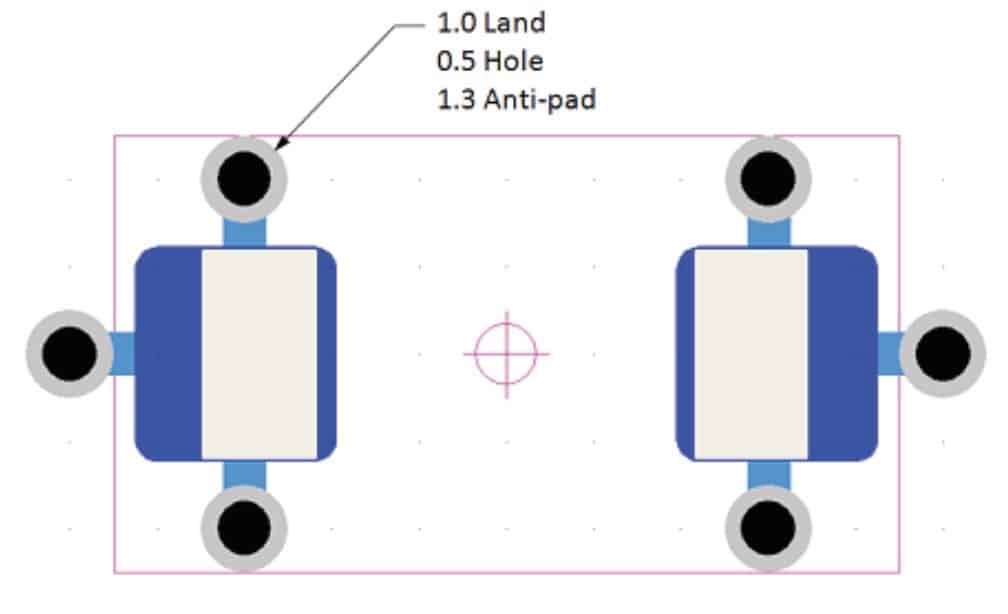
For the 7343 molded body tantalum capacitor, Figure 4, it is recommended that a larger via size,with a 1 mm land, 0.55 mm hole size, and 1.3 mm plane anti-pad, be used. The larger via can carry more current and you only need two (but the EE will ask for a 3rd one).
The illustration in Figure 5 snaps all the vias to a 1 mm grid system. These vias are twice the size of the previous vias but the same trace/space rules apply. The display grid is 1 mm. Because the land pattern, traces, and vias are on a 1 mm snap grid, this improves the copy/paste feature for manual fanout of all of the 7343 molded body components in your PCB layout.
Q: Do multiple and larger vias affect CAPM soldering?
A: The GND & PWR vias have a direct plane connection (no thermal pattern in the via hole). The thermal relief in this fanout is the trace between the Land and the via so you can have as many vias as you want as long as the total sum of the trace widths + via hole diameters connecting the land and vias does not exceed 60% of the land diameter. This is noted in the IPC-2221 and 2222 documents where it says that the total “spoke widths” should not exceed 60% of a hole diameter for a through-hole lead to prevent a cold solder joint. So be careful that you do not use multiple vias with wide trace widths.
Two vias are typically recommended for bulk tantalum capacitors. Three vias are shown in Figure 5 to illustrate the preferred via locations. Having two vias that come out of the sides of the land pattern is common because they are closer to the component leads. It is not recommend to have the vias come out of the ends of the land pattern because they are further away from the component leads. The closer the via is to the component lead, the greater the capacitance and reduced inductance. This via location tip only applies to bypass decoupling capacitors and discrete parts that are attached to the planes. It is also typical to see trace widths that are the same width as the via diameter. A 1.0 mm via diameter would have a 1 mm trace width. The picture shows a 1 mm via with a 0.5 mm trace width.
Q: For a square land, what “diameter” should be used for calculating the 60% maximum spoke width?
A: There are no rules for calculating spoke width for SMD lands. The 60% rule is in relation to the “hole diameter.”
Q: Do the two vias on the sides (Figure 3) leave a solder web between the via and the pad?
A: The vias coming out the “side” (rather than the top and bottom) of a chip capacitor to get the via as close to the component lead as possible to increase capacitance and decrease impedance. Ultimately, via-in-pad under the component lead will result in the best high-speed performance and highest component-packing density.
“Bottom only” component leads (like all the grid arrays: LGA, BGA, CGA) and fine pitch will drive via-in-pad to become more popular. The fact is that if you put via-in-pad on one part, you might as well do it on all parts because the fabrication cost does not change. i.e.: once you start to use via-in-pad, the fabrication cost automatically goes up, but it does not increase with the number of via-in-pads (unless you exceed several thousand holes). Each manufacturer is different.
Q: If there were no solder mask between the via and the pad, would solder migration be a concern?
A: All vias, on the same layer as the components, should be “tented” with solder mask. If there are only components on the top layer, then only the top-layer vias need to be tented. If there are components on both sides, then both sides should have tented vias.
Every design aspect should be considered when creating molded body components and the impactthat each feature of the land pattern has in the PCB design process. The land pattern is the starting point that affects every process from PCB layout through PCB manufacturing and assembly. There are dozens of things to consider when creating a CAD library that are often overlooked; this paper discussed the factors to consider when creating molded body component library parts. Each factor can directly affect the quality of the part placement, via fanout, trace routing, post processing, and fabrication and assembly processes.
原创文章,转载请注明: 转载自 吴川斌的博客 http://www.mr-wu.cn/
本文链接地址: PCB Design Perfection: The CAD Library Series Part 1: Molded Body Componentshttp://www.mr-wu.cn/pcb-design-perfection-the-cad-library-series-part-1-molded-body-components/
 /4
/4 
文章评论(0条评论)
登录后参与讨论