
Central Processing Unit (cpu)
Introduction:
CPU:This figure indicates a simple CPU architecture and its use of a variety
of internal data paths and control signals. Our CPU design should be based
on this architecture. It has seven parts:MAR,MBR,PC,IR,BR,CONTROL UNIT,
ALU .

Figure 1. cpu
Control unit: In the Microprogrammed control, the microprogram consists of some microinstructions and the microprogram is stored in control memory
that generates all the control signals required to execute the instruction set correctly. The microinstruction contains some micro-operations which are executed at the same time.

Figure 2. Control unit
The set of microinstructions is stored in the control memory. The control address registercontains the address of the next microinstructions to be read. When a microinstruction is read from the control memory, it is transferred to a control buffer register. The register connects to the control lines emanating from the control unit. Thus, reading a microinstruction from the control memory is the same as_executing that microinstruction. The third element shown in the figure is a sequencing unit that loads the control address register and issues a read command.
Purpose&Tasks:
The purpose of this project is to design a simple CPU (Central Processing Unit). This CPU has basic instruction set, and we will utilize its instruction set to generate a very simple program to verify its performance. For simplicity, we will only consider the relationship among the CPU, registers, memory and instruction set. That is to say we only need consider the following items: Read/Write Registers, Read/Write Memoryand Execute the instructions.
At least four parts constitute a simple CPU: the control unit, the internal registers,the ALU and instruction set, which are the main aspects of our project design and will be studied. You should determine the control signals according to the CPU architecture and your design.
Instruction Set
The instruction word contains two sections: the operation code (opcode), which defines the function of instructions (addition, subtraction, logic operations, etc.); the address part, in most instructions, the address part contains the memory location of the datum to be operated. For simplicity, the size of memory is 256× 16 in the computer. The instruction word has 16 bits. The opcode part has 8 bits and address part has 8 bits. The instruction word format n be expressed in Figure 3

Figure 3. the instruction format
The opcode of the relevant instructions are listed in Figure 4.In Figure 4,
the notation [x] represents the contents of the location x in the memory. For example, the instruction word 00000011101110012 (03B916) means that
the CPU adds word at location B916 in memory into the accumulator (ACC); the instruction word 00000101000001112 (050716) means if the sign bit of
the ACC (ACC [15]) is 0,the CPU will use the address part of the instruction
as the address of next instruction,if the sign bit is 1, the CPU will increase
the program counter (PC) and use its content 7 as the address of the next instruction.

Figure 4. List of instructions and relevant opcodes
Design ideas:
In this design, the most important part is control unit, next we will design it.
Micro programmed Control Unit
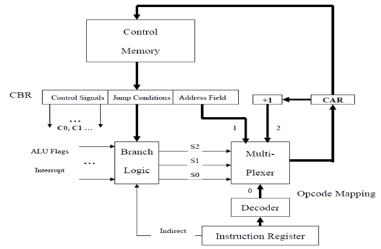
Figure 5. The architecture of control unit
The meaning of every bit of the control memory (Read Only Memery ROM) according to the requirements in our design.

Figure 6. Control Signals

Figure 7. Jump Conditions
O-----normal Ind-----indirect U------unconditional Op—map
Z-----zero M--------mpy D------div
According to the introduction We designed micro operations as follows:


Figure 8. Micro_operations
Simulated module&Contents:
The simulated ROM module

The contents in ROM(HEX):
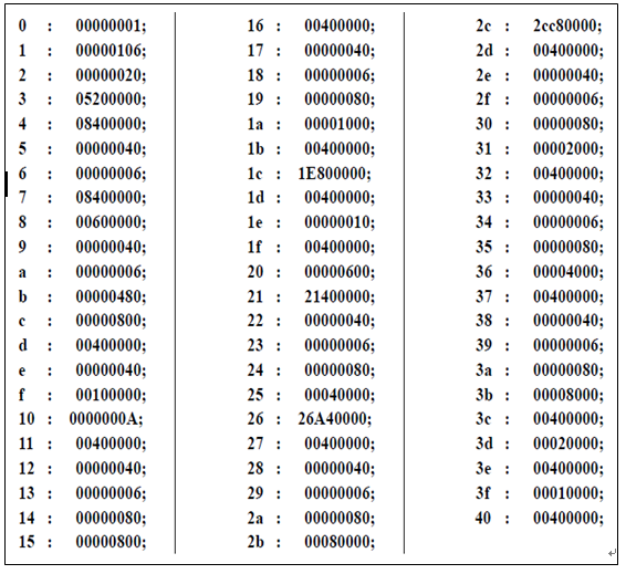
Then we complete them in the rom.mif , we write the rom.rif according to the Figure 8,it’s control signals.The results as follows:

The overall connection of the every part of CPU

our design, some operations can be supported which are listed as follows:
ADD: ACC<=ACC + BR ; SUB:ACC<=ACC-BR ; MPY:ACC<=ACC*BR
DIV:ACC<=ACC/BR ; AND:ACC<=ACC AND BR; NOT:ACC<=NOT ACC
OR:ACC<=ACC OR BR ; SRL: ACC<=Shift ACC to Left 1 bit;
SRR: ACC<=Shift ACC to Right 1 bit.


文章评论(0条评论)
登录后参与讨论