

In the wake of the Yom Kippur War of 1973, university studies in Israel were suspended, since most of the staff and students had been called up. During the hiatus, I found a job at a company called Elbit Computers, a subsidiary of Control Data Corp., a supercomputer giant at that time.
I worked in the drafting department, mainly checking that a schematic matched its associated PCB trace for trace. Even with CAD systems, I still do this today. At any rate, Control Data standards were that every IC was portrayed as at least two parts, with the first always being just the power supplies to the device. Power supplies and decoupling are vital for a circuit, but their representation on a schematic always gets in the way of the other signals, so I prefer to place them away from the rest of the schematic by perpetuating this technique.
When I produced my own schematics after that, it was by hand. I would use a logic template where I could, but anything more complex was left to my own imagination. It was difficult to replicate my own symbols, because they had been created freehand. If I wanted someone to redraw the schematic neatly, that person would have to transcribe what I had drawn -- often with mistakes.
Manual methods evolved into CAD, and I started laying out boards using a scripting language based in Autocad. A symbol involved using the graphics features and creating a table where the connections would be made. These connections would later be used to create the netlist. The collection of graphics would be combined into an entity known as an Autocad block. It was much easier to create the block as a script, because this facilitated the maintenance and copying of the symbol.
In the end, I could create such a script in my head. The package I was using (Autorouter II from the Great Softwestern Company) came with some basic symbols that were limited in number, so I was pretty much obliged to create a symbol for each part I used. During that period, I also began to appreciate the information communicated by the IC manufacturer by using symbols and pin names within the symbol. This information added to the understanding and debugging of the circuit. Because I could, I started trying to approximate the circuit representation from the data sheets. This has influenced me ever since.
As CAD improved, I moved to PCAD over several iterations -- DOS-based PCAD, then Accel (renamed PCAD), then Windows-based PCAD (back to its original name), and finally to Altium. Each version always boasted many symbols, which were either very simplistic or not to my taste. Also, I have a tendency to select parts that are not quite mainstream, and even though I consider my work to be trailing edge, I often select components that are new to the market. More often than not, the symbol is not in the library provided. Since I inevitably have to create a symbol, every time I evaluate a package, I look to see whether the symbol can be translated and how easy it will be to recreate.
At Control Data, the schematic drawing had letters along one dimension of the sheet and numbers along the other, so it was possible to localize a zone of the sheet using its matrix coordinates. (The same technique was used to locate roads, towns, and other entities on maps -- remember the days before GPS?) When a net was split on a sheet, an arrow would point to the other side of the net, and a matching arrow would point back. When the net went off the sheet, the sheet number and matrix co-ordinates were written next to the off-sheet symbol. Similar approaches were used widely throughout the industry. I remember Intel used an off-sheet convention on its SBC (Multibus) schematics. Unfortunately, this no longer seems to be practiced, and I know of no current CAD system that provides this option.
I recently purchased a development board that uses a 100-pin microcontroller (MCU). The symbol was just a square with 25 pins to a side. The schematic consisted of 15 mini-sheets. Probably two-thirds of the pins were named as nets that may or may not have connected to one or more nets of the same name on other sheets. How do you try figure out whether a pin goes to a connector or a LED on the same sheet, different sheets, or both? I don't believe this lack of information is unique to the manufacturer I was using.
Now, if you are working within the CAD package, maybe you could argue that it has tools to highlight the net in total, so that you can easily locate and work with it. But when you print the document, you don't have access to the CAD tool and are therefore SOL (sadly out of luck). Another problem, as we shall see in an example in a moment, is that CAD systems evolve, mutate, and even disappear over time. Even if your CAD system is called the same name as an earlier incarnation, it may not work with the electronic files in the same way. PCAD -- as it evolved through different owners and from DOS to Windows -- provides a prime example. In such a case, a paper copy is your only backup.
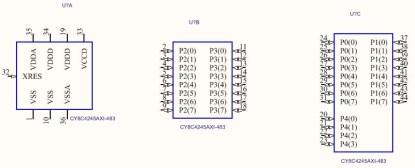
Over the years, I have designed my system to avoid disjointed nets on a single sheet and to have as few intersheet connections as possible. For a large IC, I partition it into several parts, and I try to be as intuitive as possible. Where the schematic spreads to several sheets, it is possible to place a block near the associated components. For example, one of the Cypress PSoC4 range is presented in a 48-pin package. I partitioned this as illustrated in Figure 1.

When creating symbols, I have found different CAD packages to be quirky and sometimes surprisingly inflexible on things like text orientation and style. I always prefer my text sans serif, but it is not always possible to set up a default font. Take a look at the symbols in Figure 1. Even though everything is default, there is a mix of sans serif and avec serif fonts, along with different text sizes. And try to persuade the vertical text to be horizontal. This is from Altium as it currently stands. Funnily enough, the older PCAD could do this, but it couldn't tell if a font had already been loaded, so it would load a new font for every symbol, bulking up the file size. Sigh.
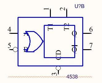
One of the problems associated with using your own symbols comes up when the software goes through an upgrade. When PCAD was discontinued and subsequently wouldn't run happily on Windows 7, my company moved to Altium, which had taken over PCAD. Promised compatibility is not always as smooth as you would hope. Figure 2 shows a monostable flip flop as it was in PCAD, while Figure 3 is the translation as seen in Altium.

I know I am old school, but I prefer it when my work looks good, and I feel it adds to the understanding of the circuit. How do you approach your symbols? Does your company have standards with which the symbols must comply?
Aubrey Kagan is Engineering Manager at Emphatec.
 /5
/5 
文章评论(0条评论)
登录后参与讨论