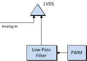


Seeing the new analogue-to-digital converter (ADC) IP being touted around by the FPGA vendors got me wondering what is behind all this. It all boils down to the fact that a comparator is, in essence, a one-bit ADC, while an LVDS I/O receiver is a comparator. Most new FPGA families have LVDS I/O as an option, and it is not hard to add a discrete LVDS RX chip to a CPLD input bank.
Thus, a programmable comparator may be created by feeding an LVDS I/O an analogue voltage. This may be a single-ended comparator. If two I/Os are employed, a window comparator may be realised. The analogue voltage may be created via a pulse-width modulated (PWM) channel within the FPGA, allowing it to self-tune the comparator. This means any unused LVDS channels can be employed for things like system monitoring or generating alarms for external conditions with the addition of signal conditioning circuits like op-amps or instrumentation amps plus sensors.

LVDS I/O used as a programmable comparator.
Though not the subject of this blog post, this also serves as the basis for many of the new ADC modules we are seeing released as IP for FPGAs. (The secret sauce is how they read the LVDS I/O and drive the PWM to achieve 12bit accuracies and 1MHz conversion rates.) A comparator is fast—400MHz or more—whereas the ADC uses more FPGA resources and is slow, but it gives resolution in bits.
The LVDS I/O will have an allowable common mode voltage range specified in the FPGA vendor's data sheet. Be sure that your design will observe this range, and don't forget to allow for the offset between the positive and negative LVDS input pins.
Also, the LVDS I/O specifies a certain amount of hysteresis, so make sure to include it in your design calculations. Again, this may vary from vendor to vendor, depending on silicon characterisation, but it should meet the LVDS specification's minimum/maximum values. This data sheet for a Maxim discrete LVDS receiver IC shows a common mode range (2.36 V) and hysteresis (50 mV) typical for an LVDS I/O.
Accuracy can be enhanced by reading calibration values from an SPI or I2C serial EEPROM into the FPGA. These can be used to store offsets, temperature calibration, voltage calibration, etc. Furthermore, the FPGA fabric or microprocessor core embedded in the FPGA can run a checksum or cyclic redundancy check on the calibration at every boot or periodically.
Even with the good hysteresis provided by the LVDS I/O, the comparator can chatter on a slow, noisy signal. If this occurs, you will need to follow it up with a good debounce circuit inside the FPGA. Here an example of a debounce logic circuit with an associated VHDL.
As I previously mentioned, a window comparator can be fashioned from two I/O channels, and this can even serve as the partial basis for a hysteretic switch-mode power-supply controller fashioned within the FPGA.
A programmable comparator may drive a counter/timer module in an FPGA. It may also serve as the basis for a built-in self-test (BIST) for a multi-clocked design. A multiplexer can feed signals into the counter/timer module and allow measurements of things like clocks, synthesisers, and other Analogue/RF/IF components to be read back into the FPGA for test.
The LVDS I/O in the FPGA can also be used as programmable logic threshold I/O for legacy digital IC compatibility applications. Any logic threshold within the vendor's LVDS common mode range that the I/O will support can be set via the PWM, allowing plug-and-play capability with legacy systems. This lets you create a variable threshold FPGA logic analyser for BIST or other applications.
One could also use the comparator to create a one-shot or mono-stable mutivibrator for a special application. Regular multi-vibrators or programmable oscillators are another possibility, while voltage controlled oscillators and alignable Xtal (crystal) oscillators could be used to build special pressure and temperature sensors.
Have you used any of these techniques—or similar or related ones—in your FPGA designs?
William Murray
Electrical Engineer
 /5
/5 
文章评论(0条评论)
登录后参与讨论