Key words:TFT, thin film transistor, key drive device of LCD (driving orientation of liquid crystal molecules) and AMOLED flat display (driving OLED)a-Si, amorphous silicon, very early technology of TFT in FPD
LTPS, low temperature poly silicon, much higher electron mobility, particularly used in mobile display applicationsFPD, flat panel display
CD, critical dimension
CF, color filter, the 2nd glass in LCD
ESA, electrostatic attraction
ESD, electrostatic discharge
LCD, liquid crystal display
AMOLED, active matrix organic light emitting diode1.Brief view on electrostatic problems in FPD manufacturing: Electrostatics-induced-electrical failures, particle contamination and process control errors
Electrostatics in FPD manufacturing is very common seen and could induce remarkable impacts to the whole FPD industry. It mainly includes three portions listed as below.
Firstly, electrostatics-induced-electrical failures of FPD products is the top concern, typically TFT array circuits formed on glass substrates. These electrical defects both includes functional failures caused by catastrophic damages which directly impact production yields, and latent failures (or called “wounded walking”, typically are those gate oxide dielectrics, interlayer dielectrics or passivation) which may not impact production yields throughout FPD manufacturing, however, the reliability of these FPD products would be degraded and may lead to lower robustness to ESD in the following manufacturing processes or earlier failure in reliability testing or even at end-users’ applications.
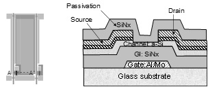

Fig1. Typical structure of bottom gate a-Si TFT (left) and top gate LTPS TFT (right)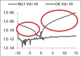
Fig2. Typical electrical failure caused by electrostatics induced ESD: higher gate leakage at electrical testing The other part could be impacted by electrostatics is the photomask used as a key process tool in photo-lithography process-exposure equipment. Electrostatics could also lead to physical damages (typically Critical Dimension failures) to the large amount of isolated chrome patterns deposited on glass or quartz substrates. Photomasks with CD failures if input into exposure equipment for production would produce lithography errors and lead to failed TFT glasses at very high possibility. This would be a disaster to any FPD manufacturer.
Secondly, electrostatics induced particle contaminations to FPD device (including TFT deposition layer contaminated, glass substrates contaminations) and processing materials (such as photo-resist contaminated, susceptor surface contaminated of CVD, PVD, Dry-etching equipment). The effect of electrostatic attraction (abbr. ESA) dominates this type of particle contamination where cleanroom environment especially for the mini-environment inside manufacturing equipment with over-more airborne particles.
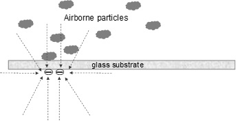
Fig3. Local electrostatics on glass substrate attract airborne particles to case contamination
Fig4. Actual case of TFT array glass contaminated by particles
Lastly, electrostatics could also impact on process control qualities. For example, poor uniformity of liquid crystal molecules filling in ODF (One Drop Filling) process. Another example is misalignment between CF glass and TFT glass in vacuum assembly process.
2.Electrostatic Devices and the Sensitivity to Electrostatics: TFT array pattern and photomask
Regarding electrostatics induced electrical defects, TFT array patterns of FPD products formed on glass substrates and chrome patterns formed on glass or quartz substrates.
TFT array patterns consists of large amount of multi-layer devices over one glass substrate. It’s sensitivity to electrostatics in manufacturing is quite similar with wafer fabrication processes of semiconductors. That is insulating dielectrics between metal lines or between metal and poly silicon are susceptible to be damaged by electrostatic impacts, and dielectric leakage and lower electrical reliability are the main failures. However, FPD products would be exposed to many more and high electrostatic impacts because of the insulating glass substrates. On the other hand, FPD TFT array patterns consists of many much longer metal lines which would attract the electric fields and amplify field strength. Therefore, electrostatics induced electrical defects of FPD manufacturing is much worse than wafer fabrication of semiconductor.
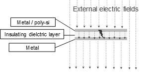
Fig5. Typical electrostatics sensitive device model in TFT array patterns of a FPD product

Fig6. Electrostatics-induced-electrical failures by ESD on a mother glass substrate at TFT array fabricationThe sensitivity of FPD TFT array patterns to electrostatics could be described as below:Electrostatic sensitive device pattern of metal/polysilicon-dielectrics-metal structure, while exposed to electrostatic sources, there would produce an electric field applied across the dielectrics.The higher strength of the electric field applied across the dielectrics, the higher probability of the dielectrics to break down (higher mobility of electrons). An abrupt discharge current would flow through the dielectrics if the field strength exceeded the breakdown threshold of the dielectrics (eg. Common gate insulation layer of TFT is SiO2 or SiNx, the electric breakdown threshold is about 5-10 MV/cm), and finally a leakage path would form across the dielectrics which is the electrical leakage failure.The sensitivity of photomask to electrostatics is similar with FPD array patterns, since both have similar electrostatic sensitive device pattern, similar sensitivity mode to electrostatics and similar electrostatic sources in manufacturing. The major difference of photomask is chrome-air-chrome structure only which could be damaged by electrostatics.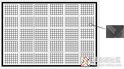
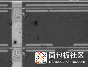
Fig7. Typical chrome pattern CD failure of FPD TFT photomask caused by electrostatics induced ESD3.Process flow of FPD ManufacturingFPD manufacturing consists of three sections, the front-end TFT array fabrication (and CF fabrication for LCD), the mid-end cell assembly for LCD & OLED evaporation, encapsulation for AMOLED and back-end module assembly.TFT array fabrication almost share the same manufacturing processes with wafer fabrication of semiconductor. TFT array fabrication also consist of thin film process by CVD & PVD, photo process, wet etch & dry etch, and stripper and similar equipment but lower-class. However, TFT fabrication has more transferring processes by robot arms and long conveyors of rolling rollers which could produce many more electrostatics to impact FPD products.
Fig8. Typical manufacturing processes of TFT array fabricationLCD cell consists of PI coating, PI baking, PI rubbing of both TFT glass and CF glass, seal dispense of TFT glass, spacer dispense of CF glass, ODF of TFT glass and vacuum assembly of LCD cell. All these processes would involve transferring glasses or pick and place of glasses which all are prone to accumulate electrostatics.
Fig9. Principle manufacturing processes of LCD cell assembly
OLED evaporation consists of many vacuum chambers to process and transfer glasses where highly electrostatics could be a common problem.
Module assembly consists of several thin film attachment including Polarizers, protective films which could accumulate large amount of electrostatics in peeling and attachment operations.
4.Electrostatics in FPD Manufacturing
Electrostatics in front-end and mid-end FPD manufacturing mainly comes in several conventional ways:
Contact and separation tribo-electrification (or called tribo-electrification) between equipment part and FPD glasses, such as pad-glass in robot arm to transfer glasses from one location to another, roller-glass in rolling transfer glasses, stage-glass in glass processing on equipment stage/chuck/susceptor and rubbing cloth-PI on glass in PI rubbing process.
Fig11. Contact and separation electrification (tribo-charging) of glass on an equipment stage
Fluid charging (or called electrification) is another important way to accumulate electrostatics on TFT array glasses, including highly purified water jetting rinsing, spin drying after water rinsing, photo-resist slit coating, PI coating, liquid crystal molecules dropping in ODF, etc.
Plasma (vacuum and atmosphere), Ultraviolet (Extreme-UV and Excimer-UV) exposure or irradiation could also produce and accumulate electrostatics, such as plasma of CVD & Dry-etcher, dry cleaning by atmosphere pressure plasma, dry cleaning by excimer UV, etc.
It should be noted that the above ways to accumulate electrostatics could show variations by process setup or equipment individual condition.
For example, the tribo-charging by contact-separation way on a vacuum stage of exposure equipment varies by different equipment settings. Vacuum pressure, vacuum holding time duration, glass lift-up speed, etc. each could produce tribo-charging amplitudes of glass substrates. Moreover, the contact-separation tribo-charging could get worse as the exposure equipment continue to process more and more glasses.
Another example is the conveyor line of rolling rollers. The tribo-charging between glass bottom side and rollers would produce more electrostatics accumulated on glass bottom side as transferring over longer distance. Common rollers made with materials of Teflon, PVDF, UPE and stainless steel could produce varied tribo-charging amplitudes and accumulation speeds over rolling transferring. To resolve electrostatic problems in FPD manufacturing, many manufacturers attempted to enhance roller’s conductivity by adding different conductive additives. These modified rollers would also show different tribo-charging of glass substrates.




 /2
/2 
文章评论(0条评论)
登录后参与讨论