

Some 99 percent of the "design" problems associated with linear and switching regulators can be traced directly to the improper use of capacitors: wrong type, wrong value, or incorrect physical placement. Regulator designs sometimes diagnosed as "unstable" are often simply victims of bad layout or inadequate bypassing. Excessive EMI is frequently caused by poor bypassing and failing to snub high-frequency noise generators at the source. This article will cover some of the most common mistakes made and provide solutions.
Switching regulators
The switching regulator is inherently vulnerable to poor capacitor design methodology for the simple reason that all switching regulators draw high peak currents when they switch on. The fundamental question is: Where will that current come from? The answer is a capacitor, and that capacitor had better be a very good one with a minimum amount of inductance between itself and the switch or all kinds of problems will result.
Local bypassing
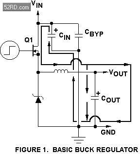
The basic buck regulator circuit in Figure 1 will be used to illustrate the single most common design mistake made in switching converters: inadequate input support capacitance (sometimes called "local bypassing" because the input capacitor CIN keeps the switch currents confined to a local area on the board). If the input support capacitor is either too small, too far away, or simply not good enough in high frequency performance to provide the switch peak current, there will be serious problems.
When the main switch Q1 turns ON, current must flow along the path shown by the arrows. For the regulator to operate efficiently, there must be a minimum of switching losses which requires a very fast rise time for the current. This current can only be provided by CIN, and that requires that it be a very good high-frequency capacitor with low impedance. Because a fairly large amount of capacitance would be required, this cap would likely be a Tantalum or Aluminum electrolytic designed for HF switching. Of course, the best capacitor in the world is useless if the trace inductance between it and the switch FET is large enough to cause limitations of the rise time of the current. For this reason, all of the power components in a switching converter must be kept physically close and trace inductance kept to a minimum.

RF noise bypassing
When a switch is used to chop a voltage provided by a DC source, a significant amount of noise will be put onto that DC line by the switching converter. To minimize the noise conducted back to the rest of the circuitry through this line, good bypass caps are essential. In Figure 1, it was shown that CIN was used to supply the high peak currents to the FET switch.
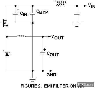
The Tantalums and aluminum electrolytics typically used for CIN become fairly reactive at higher frequencies (above a few MHz) because of relatively high ESR (equivalent series resistance) and ESL (equivalent series inductance), and are therefore poor RF bypass capacitors. As shown in Figure 1, CIN must be paralleled by a good ceramic capacitor CBYP for RF bypassing to reduce the amount of hash that will be conducted back on the DC source line to other circuitry. Amount and type of capacitor(s) used on the input line of the switching converter is basically application dependent. In some higher current converters, the amount of RF noise on the VIN line at the switching converter input is so high that simply bypassing to ground does not provide enough noise reduction. Then it becomes necessary to add an L-C filter as shown in Figure 2 to prevent this RF from causing problems in other circuitry powered from the same source. It is not always necessary to add a physical inductor to achieve noise reduction, sometimes trace inductance can be used effectively to reduce high frequency noise in conjunction with good ceramic bypass caps placed near the VIN pins of the devices which require clean power.

Snubbers
Without question, the best way to handle the problem of RF EMI is to minimize or reduce it at the source. In switching converters, the source of the nastiest EMI is usually the power switch (FET) and the worst EMI is usually when it turns OFF. To understand why, simply refer to figure 1: when QI is ON, current flows through the inductor. When Q1 is turned OFF, the voltage on the FET end of the inductor is forced to swing negative until the diode turns ON to hold the current through the inductor constant. A silicon ultra-fast diode can not turn ON in zero time, so the voltage can shoot negative beyond a diode drop and then ring as the diode turns ON.
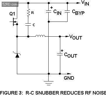
Even if a Scottky diode is used, parasitic trace inductance will still cause some ringing to occur. This ringing is usually in the 20 MHz to 100 MHz range and generally seems to appear on every circuit node in the lab within ten feet of the board under test. It is “seen” everywhere because the EMI induces a signal directly into the scope probe''s ground lead. A good way to reduce this EMI is to add an R-C snubber as shown in Figure 3 (typically a ceramic capacitor and carbon film resistor). It works because when the FET stops sourcing current, the capacitor will source enough current so that the di/dt rate of current fall through the inductor is not as fast. The R-C also damps out the ringing if the component values are appropriately selected. Snubbers have the disadvantage that they reduce overall efficiency by a few percentage points. The loss of efficiency shows up most at light loads because the power they burn is basically constant and relatively independent of output load current, which means the percent of total converter input power consumed by the snubber increases at lighter loads.

Ripple current
The single most commonly made mistake in component selection for capacitors in switching regulators may be in the ripple current specification. Ripple current is the RMS value of the current flowing into and out of the capacitor each time the switch turns ON and OFF. Referring to Figure 1, there is a ripple current flowing in both CIN and COUT. Current flows into and out of CIN as the FET turns on and off, and current flows into and out of COUT as the inductor current charges it and then the capacitor discharges into the load. What must be understood is that the ripple current flows through the ESR (equivalent series resistance) of the capacitor and dissipates power as given by the well known term for power which is:
P = I(squared) * ESR.
Ripple current derivations are not trivial in many switching converters and some designers have been known to solder a 10 milli-Ohm resistor on the ground side of the capacitor in question and snap a scope photo to see what the ripple current actually looks like. Then, a graphical estimate of the RMS value gives a good approximation. The only definitive test of the capacitor selected is to check the temperature rise when operated at full output load current. What is most important to realize is that if you replace a good, high-frequency low-ESR switching cap with a generic aluminum electrolytic it will likely overheat and fail due to the increased power dissipation caused by the ripple current.
Linear regulators
A dangerous precedent was established by the first linear regulator semiconductors sold commercially like the LM7805 type devices: they require no input or output capacitor and are completely stable under virtually any operating conditions. Some of the newer LDO regulators require careful attention to external capacitors to operate in a stable mode. The main reason the 7805 is unconditionally stable is because the power pass transistor was made up of an NPN Darlington as shown in Figure 4. They are usually referred to as “NPN regulators” for this reason, and are comprised of an error amplifier, voltage reference, and NPN Darlington power transistor.
The NPN regulator drives the load off of the emitter of an NPN transistor in a configuration sometimes called “emitter follower” because the voltage gain from base to emitter is nearly unity, but the current gain is very high. The critical characteristic of the emitter follower is that it is very wide-band and does not introduce low-frequency poles into the loop gain. This makes compensation very easy: “dominant pole” compensation is used by putting a pole into the loop created by the capacitor around the error amplifier. The result is a very low frequency pole (typically around 10 - 100 Hz) causing a 20 dB/decade roll-off out to the unity gain crossover frequency which is typically between about 100kHz and 1 MHz. This shows why no external compensation is required for stability in an NPN regulator.
LDO regulators
NPN regulators are a great product, but as the voltages used in circuits have dropped lower, they have become less attractive because of one reason: dropout voltage. This is defined as the minimum voltage (input-to-output) which must be maintained for the regulator to hold the output in regulation. The standard NPN regulator requires about 2 - 2.5V minimum because of the 2 VBE''s + 1 SAT required to operate the NPN Darlington power transistor and PNP driver. The power dissipation caused by the voltage drop across the regulator becomes more and more significant as the regulated output voltage drops. This led directly to the development of the LDO (low dropout) regulator which can operate with as little as a few hundred millivolts across it (see Figure 5).
The LDO regulator (sometimes called a “PNP” regulator) differs from the NPN regulator because the power transistor is a single PNP: the good news is that dropout voltage can be as low as the saturation voltage of the PNP (a few hundred millivolts). However, the single PNP has lower beta compared to the NPN Darlington, so the ground pin current of the LDO regulator is approximately equal to the load current divided by the beta of the PNP. To reduce this current, very good PNP devices have to be fabricated on the IC which have high current gain. The VIP devices used on our LP298X line have typical betas > 100 so the ground pin current is kept very low.
The major difference between the LDO and the NPN regulator is that the LDO must be compensated differently from an NPN regulator. The LDO requires an output capacitor, and the ESR (equivalent series resistance) of that capacitor is integral to stability. The reason for this is because the PNP drives the output off the collector (in a configuration called common-emitter) and has a fairly high output impedance. Because of this, the loop gain has a pole in it (I will refer to as the Load Pole) formed by the output capacitor and the load resistance. The load pole frequency is closely approximated by:
fLP = 1 / (2 * pi * RL * COUT).
The presence of a second low-frequency pole poses a problem: two poles can result in 180 degree phase shift which will cause oscillations. The solution is to introduce some positive phase lead to cancel out some of the shift from the two poles. This is accomplished using the ESR of the output capacitor. A zero is created by the ESR whose frequency is given by:
fz = 1 / (2 * pi * ESR * COUT)
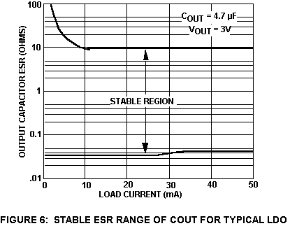
If the ESR is in the correct range, stable operation will result because it will provide enough phase lead to get sufficient phase margin at the unity gain frequency. If the ESR is too low, the zero doesn''t kick in until well past the unity-gain frequency so it does no good. If the ESR is too high, the zero comes in at too low of a frequency and the loop bandwidth will get too wide (and that allows other high-frequency poles to add phase shift and cause oscillations). So, it has to be in the right range. The way we determine the range is to bench test the regulator using a capacitor which has pretty close to zero ESR (surface mount ceramic) and add series resistance values and plot ESR stability curves (Figure 6).

本文来自:我爱研发网(52RD.com) 详细出处:http://www.52rd.com/S_TXT/2005_9/TXT1901.htm
 /3
/3 
文章评论(0条评论)
登录后参与讨论