今天给大家介绍一下Spacer(侧墙)模块以及LDD(浅掺杂漏 & Halo(晕环) IMP模块。
-
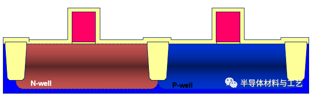
Spacer1 Formation
在沉积Spacer前,先做一道 Wet Clean,然后用furnace的方式长一层40A左右的Ox(Poly Reox),接下来继续Dep一层Offset Spacer Ox。
Q:What is the purpose for poly Reox?
A:Poly reoxis to repair damage during gate etch, improve GOX quality at poly edge.
-
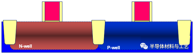
Spacer Etch
刻蚀掉poly顶部和有源区的Ox,留下poly两侧的Ox。
Q:What need offset spacer?
A:1.To enlarge gate to drain Overlap Capacitance to improve MOS AC performance
2.In 65nm process, SCE is very serious. Too much gate to S/D overlap will induce high Ioff.
3. Pre-Amorphization Implant(PAI):预非晶化注入
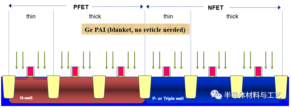
在做LDD IMP之前先打一道blanket Pre-Amorphization IMP.
Q:Why need PAI?
A:1.PAI implant is performed after poly gate/offset spacer1 formation.Amorphize the poly gate and source/drain region.
4. reduces channeling of subsequent implant steps → LDD, Halo, Source/Drain.
-
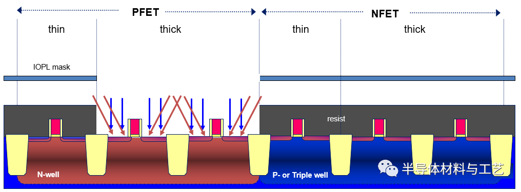
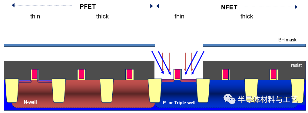
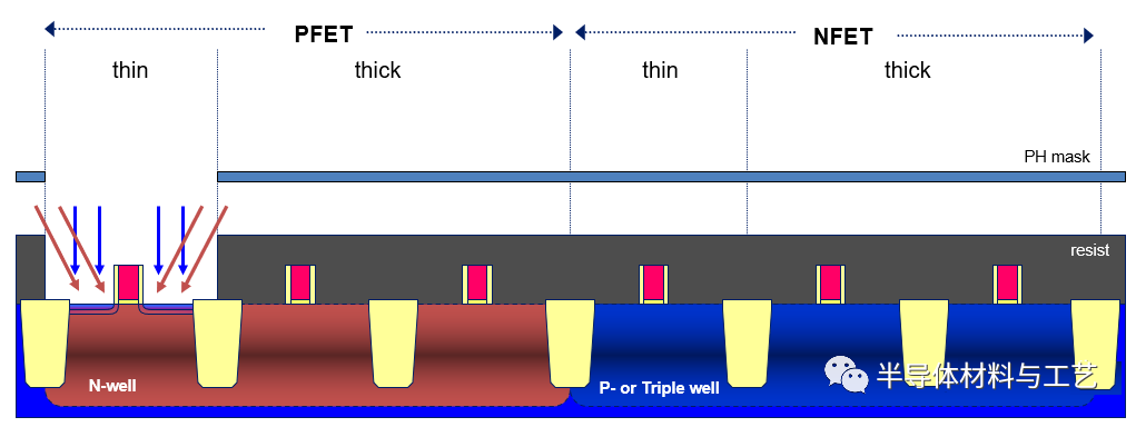
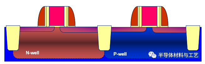
LDD(Extension) & Halo(Pocket) IMP
IO区的NMOS LDD&Halo IMP
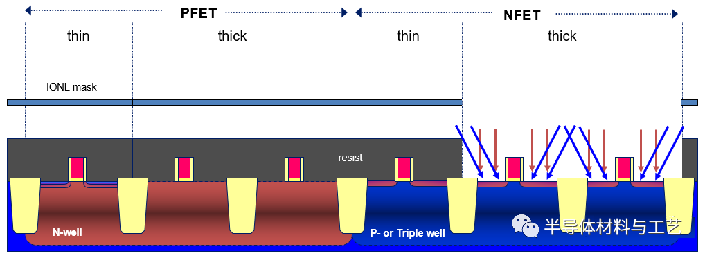
LDD IMP是为了减小漏极附件的峰值电场,达到改善HCI(Hot Carrier Inject)效应和器件可靠性的目的。
Halo IMP的作用是防止低压短沟道效应。
如下分别在Core区和IO区对NMOS和PMOS进行LDD&Halo的IMP。
IO区的PMOS LDD&Halo IMP
Core区的NMOS LDD&Halo IMP
Core区的PMOS LDD&Halo IMP
拔完光阻,接下来做Spacer2的Dep.
5. Spacer2 Formation
先Dep一层LTO(低温氧化层,Reduce thermal for shallow junction ),然后继续用PECVD的方式Dep一层SiN,形成类似“蘑菇头”形状的结构。
6. Spacer2 Etch
用干法刻蚀的方法,去掉poly顶部和有源区的SiN,留下poly两侧的SiN.
7. S(Source)/D(Drain) IMP
PMOS的S/D IMP(此处有时会做一道PAI),有的技术会加打fluorine,目的是为了improve NBTI.

PMOS的S/D IMP
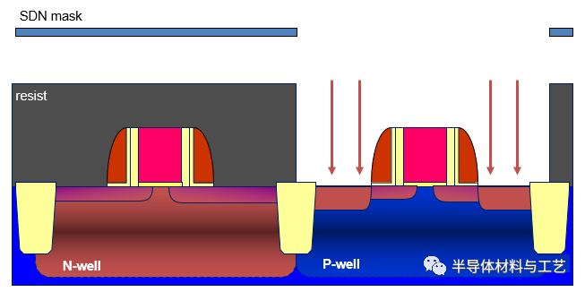
S/D IMP结束拔完光阻,做下一个模块SAB.
注:1.在更先进的工艺里在Spacer1与SPacer2工艺之间还会有EPI(外延硅:SiGe/SiC)工艺。这个以后给大家分享28/22nm工艺时再详细讨论。
2.在更先进的工艺里S/D与SAB模块之间还会有SMT(Stress Memories Technology)技术。之后会出专题专门介绍一下SMT技术和侧墙工艺(Spacer Sidewall)的“来龙去脉”。
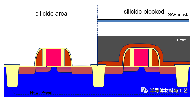
(一).SAB( Self Aligned Silicide Block自对准金属硅化物阻挡层)工艺
-
LTO & SiN DepS/D IMP做完后,继续Dep 一层LTO(低温氧化层),然后进行Spike Anneal(和S/D的Anneal merge在一起,降低thermal)。用PECVD的方式沉积一层150A左右的SiN,接下来用PR遮挡住non-silicide的区域。
2.PR Strip & Oxide Etch
用O2和HF分别拔掉PR和Ox,然后用PVD的方式沉积Ni金属。
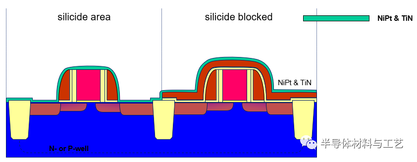
3.NiSix Anneal(Double)
Ni沉积完通过第一次Anneal1形成高阻态的NiSix,然后去除多余未反应的metal Ni,接下来进行第二次Anneal2形成稳定低阻态的NiSi2 silicide.
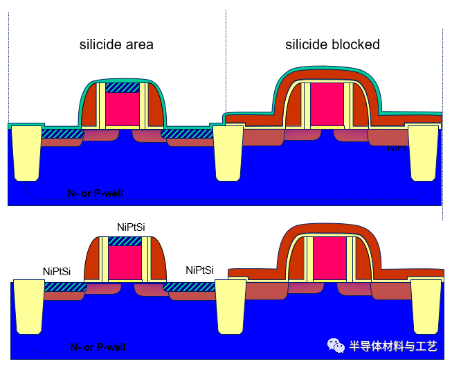
Q:Why do we need to split the anneal into 2 steps?A:The first anneal is to form Ni2Si. Then, unreacted nickel will be removed by metal strip. Subsequently, the second anneal is to convert NiSi2 into the desired NiSi (nickel monosilicide). If we attempt to convert it to NiSi with a single anneal, excessive silicidationmay occur Þleakage
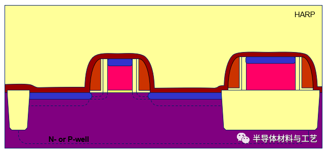
(二).ILD Module
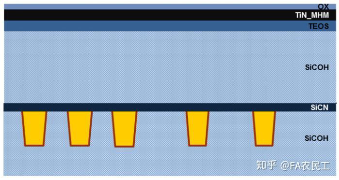
ILD:Inter Layer Dielectric 层间介电层ILD工艺是指在器件与金属1(Metal 1)之间填充的介电材料,形成电性隔离,可以有效地隔离金属互联线与器件,降低金属与衬底之间的寄生电容,改善金属横跨不同的区域而形成寄生的场效应晶体管。ILD的介质材料一般是氧化硅。ILD Dep
用HARP的方式Dep一层大约8000A左右的Ox,然后通过CMP磨掉大约4000A的Ox,再过一道Wet clean。
65nm后段工艺 (来源:知呼 FA农民工)
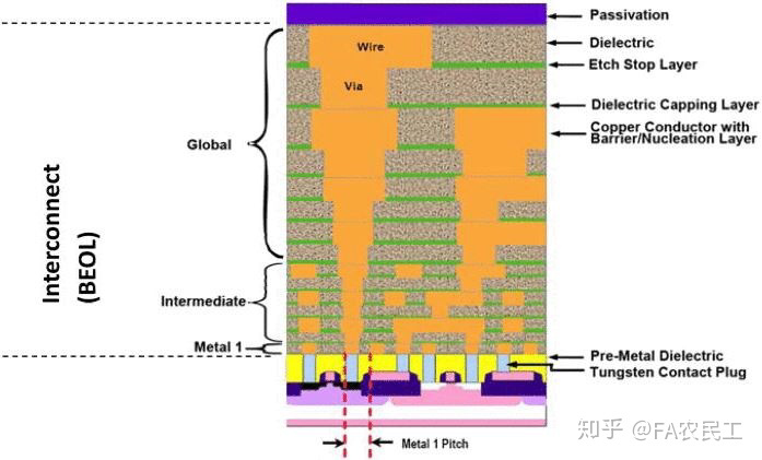
M1的全称为Metal One,字面意思是金属层1,位于中段工艺 接触孔之上。整个M1工艺中又细分为薄膜沉积→曝光显影→硬掩模刻蚀→刻蚀→种子层沉积→铜电镀→化学机械平坦化 中段工艺结束后的Wafer
 薄膜沉积
薄膜沉积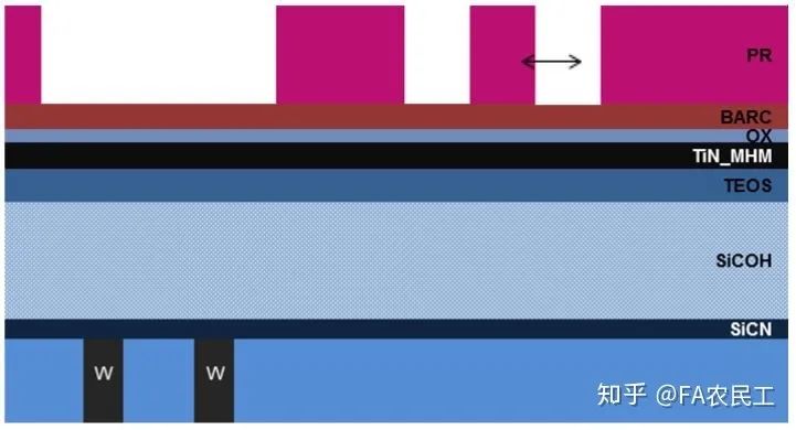 曝光显影
曝光显影 硬掩模刻蚀
硬掩模刻蚀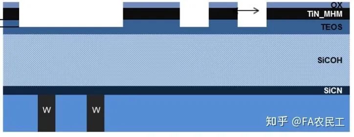
 刻蚀
刻蚀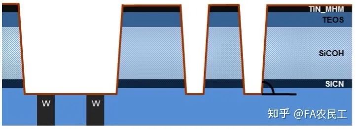 种子层沉积
种子层沉积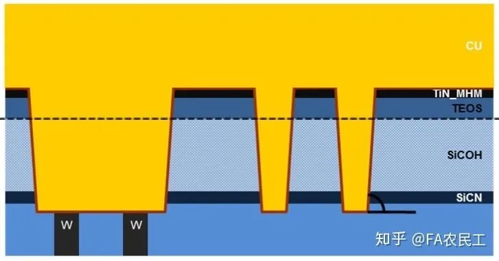 铜电镀
铜电镀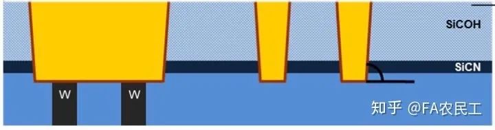 化学机械平坦化下面为每个步骤的详细介绍
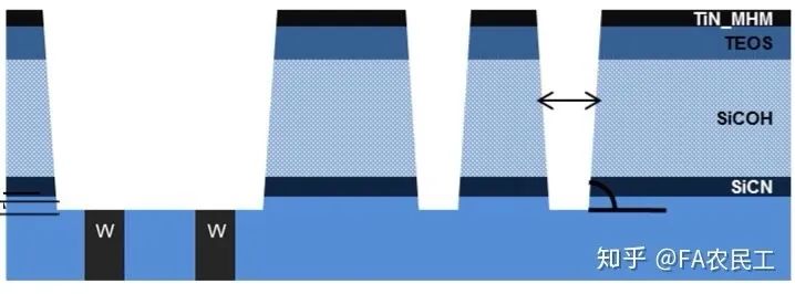
首先是薄膜沉积
从下到上依次沉积1.SiCN起到刻蚀停止层的作用2.SiOCH Low-K材料,作为金属间的介电材料3.TEOS硬掩模,起到覆盖Low-K材料及曝光图形转写的作用4.TiN 金属硬掩模5.Oxide上述5层薄膜中都采用了PECVD(等离子增强化学气相沉积)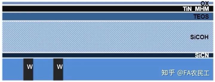
其次是曝光显影
1.对Wafer进行清洗2.旋涂BARC(抗反射涂层)和光阻3.曝光显影
接下来是刻蚀
首先进行硬掩模(HARD MASK)刻蚀Hard Mask起到了转写光阻图形及提高对下层图形选择比的作用,篇幅有限,在此不做更多说明1.打开TiN 金属硬掩模2.在原位对上层的光阻进行灰化剥离,在此步骤中会有一定的硬掩模(TEOS)损失3.清洗刻蚀副产物以上步骤完成了光阻到硬掩模的转写,接下来进行M1层的刻蚀1.LOW-K层和SiCN层刻蚀,这里有几项参数特别需要注意,分别是ILD(层间介电质)损失量,TiN残留量,侧壁的角度2.清洗晶圆表面的刻蚀副产物接着是金属沉积
1.PVD沉积一层TaN/Ta阻挡层,防止后续沉积的铜进入其他被覆盖的膜层(SiCOH等)2.PVD沉积一层铜籽晶层,此处要注意材料充分沉积在图形表面,并且不会在角落处悬挂过多,导致后续铜电镀有空隙
最后是铜电镀&CMP
电镀铜CMP(化学机械平坦化)磨去部分铜/全部的硬掩模(TiN+TEOS)以上是65/55nm后段工艺流程中的Metal1工艺介绍。
回顾一下上面提到的Metal one,即图中的Metal1,负责将下层的器件与上层的金属互连进行连接。本次将为大家介绍Metal one上Intermediate层的制造工艺流程
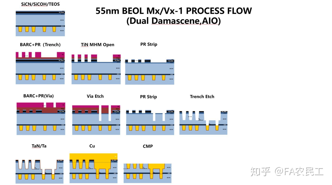
主要的工艺步骤分为薄膜沉积→AIO(Trench & Via)刻蚀→铜电镀→CMP
第一步是薄膜沉积
沉积的膜层与METAL 1一致SiCN层 刻蚀停止层SICOH层 层间介电质TEOS层 硬掩模TiN层 金属硬掩模Oxide层
第二步是AIO刻蚀
AIO=All in one 即 Trench & via 在一步内进行刻蚀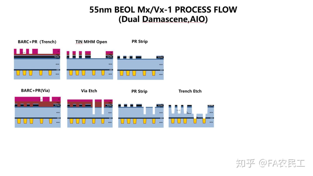 AIO1.曝光显影 ,形成Trench的图形
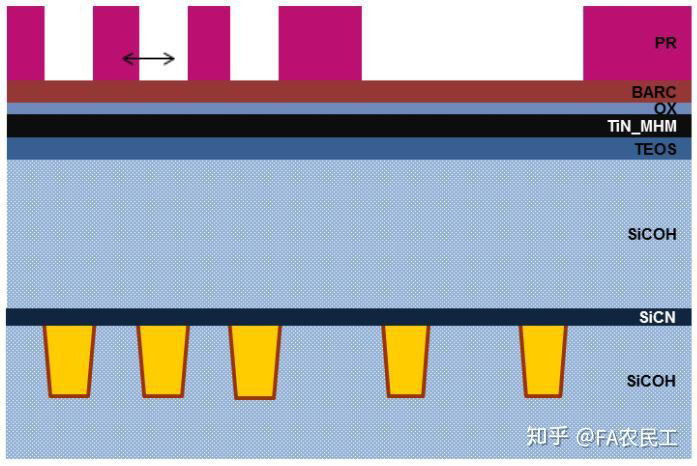 2.刻蚀打开TiN金属硬掩模,将光阻上的图形转写到硬掩模上
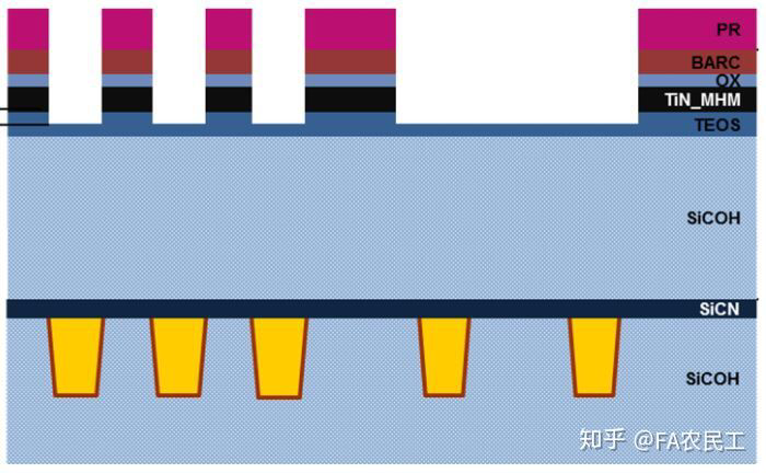 3.在原位对上层剩余的光阻和底部抗反射图层进行灰化,剥离
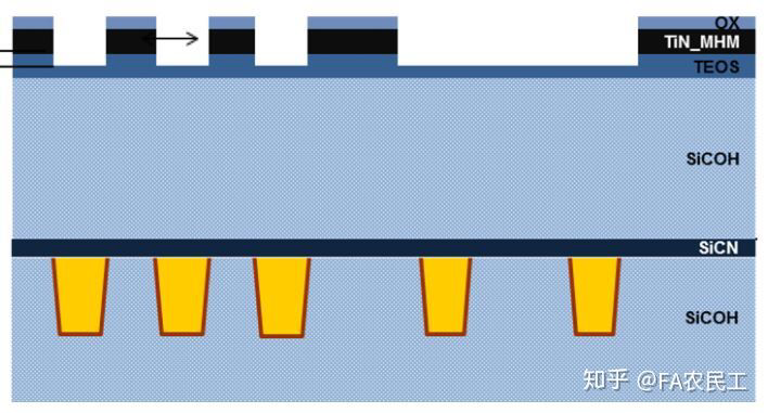 4.再次进行曝光显影,这一次的目的是形成Via的图形5.刻蚀出部分的Via图形
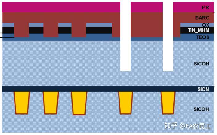 6.原位灰化&剥离光阻后,继续刻蚀形成全部的Trench & Via图形
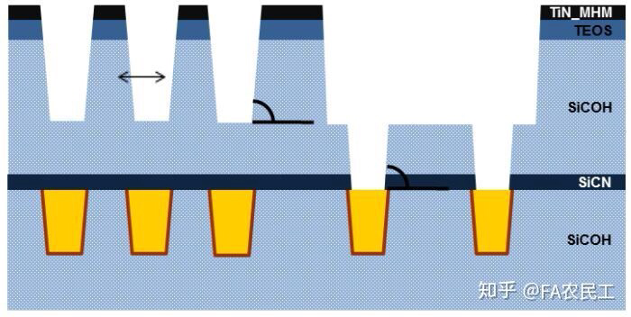 上部较大的图形为Trench下部与Metal 1相联的图形则为Via
第三步是金属沉积
沉积Ta/TaN阻挡层,方式后续电镀的铜进入到其他膜层中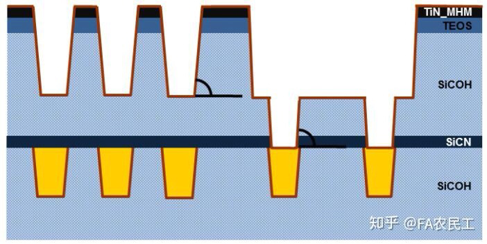
第四步是铜电镀&CMP
电镀铜填满所有的沟槽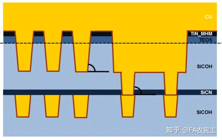 化学机械平坦化磨去SiCOH膜层上部的铜
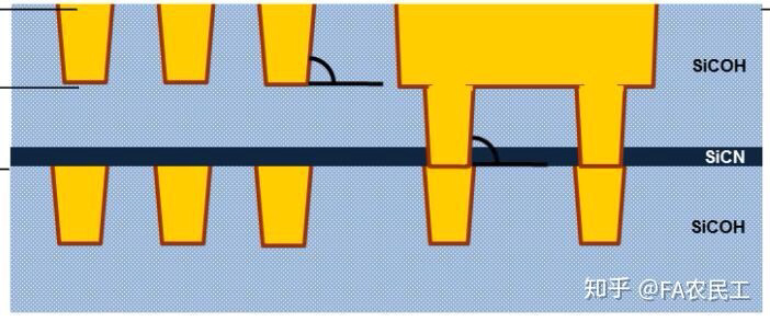 至此完成了intermediate层的工艺流程
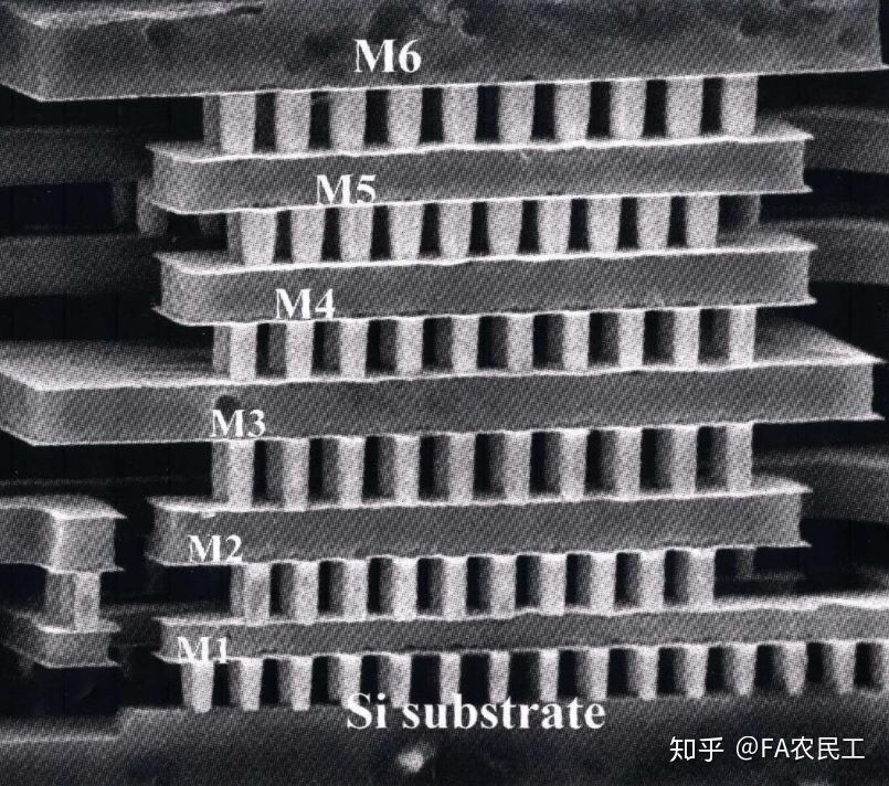 此层中的金属层数量一般为2~6层
 0
0