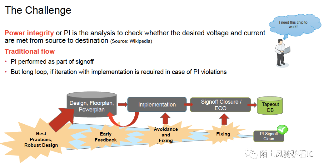
"Power has to feed every transistor within a chip. That power is distributed around the chip using the metal layers. As fabrication technologies have become smaller, the size of the wires has also been getting smaller, while physical chip dimensions have stayed roughly the same. This means that wires have become thinner but have not gotten shorter. That leads to an increase in resistance per unit length. There is an almost 10X increase in resistance between a 28nm chip and a 7nm chip, and that will follow an exponential increase for smaller geometries. At the same time, the total power consumed by chip has also remained fairly flat.
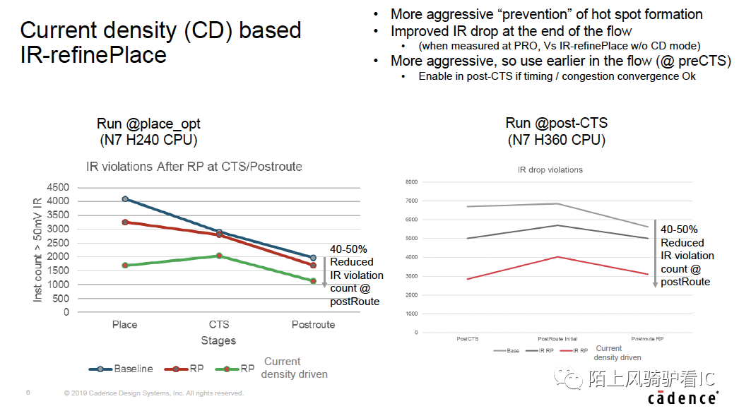
As current flows through a resistor, the voltage drops – this is what is referred to as IR drop. When the voltage at a transistor drops, it becomes slower and this could impact the circuit timing. When this happens on a critical path through a design, it can also lead to a functional failure and thus needs to be avoided. Another trend in semiconductor design has been a reduction in operating voltage, meaning that small changes in supply voltage may represent an increasing percentage of the digital swing and potentially lead to incorrect logic values being seen.
A second problem is intertwined with IR drop: electromigration. When large currents flow through these thin wires, molecular displacement can happen. This means that molecules of the metal migrate along the wires over time, causing a further shrinking of the wire at certain points and thus an increase in the resistance. So, over time, electromigration can make IR drop worse. It thus becomes necessary to analyze for IR drop over the intended life off the device coupled with electromigration analysis.
IR drop, while causing an increase in delay for a digital transistor, can have an even bigger impact on analog circuitry. Not only can timing change, but it can directly cause functional failures. Given that the current draw of a wire is influenced by activity in other areas of the chip, it is often seen as a source of noise for the analog circuitry and this has to be taken into account when doing circuit analysis."
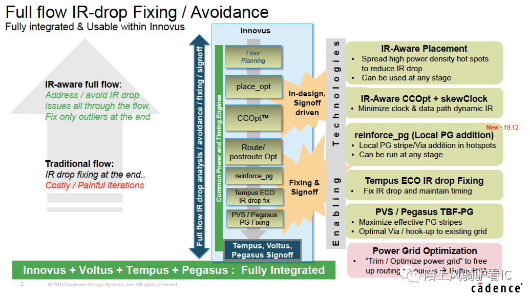
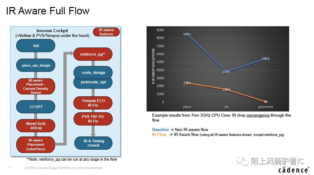
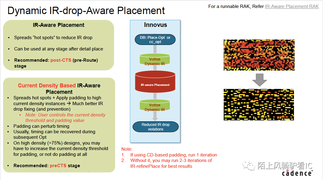
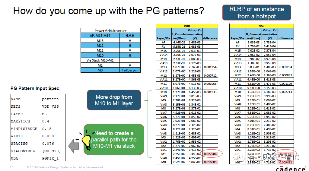
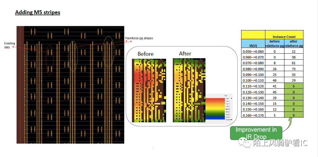
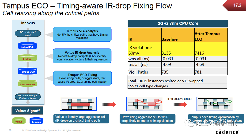
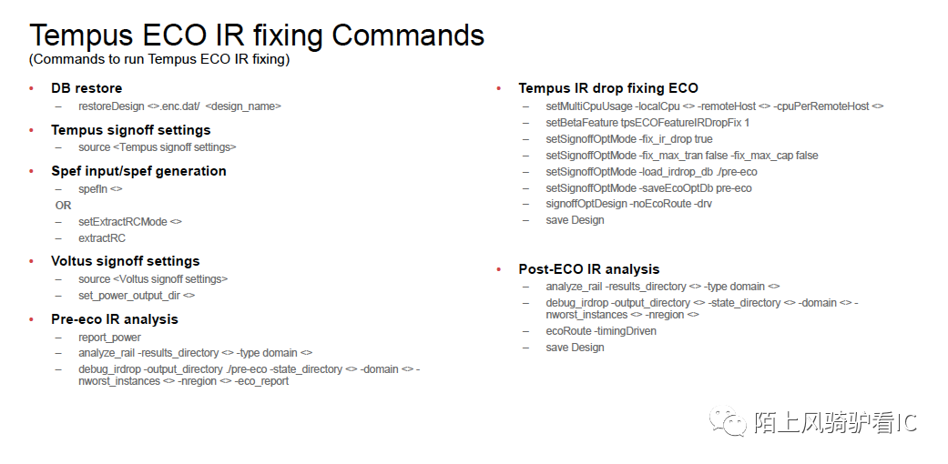
参考文献:https://support.cadence.com/apex/ArticleAttachmentPortal?id=a1O0V000009MqknUAC&pageName=ArticleContent&oMenu=People%20who%20viewed%20this%20also%20viewed
本文源自微信公众号:陌上风骑驴看IC,不代表用户或本站观点,如有侵权,请联系nick.zong@aspencore.com 删除!


 0
0


