笔者和杨帅锅一样,在入门电源的时候,不约而同地接触到了Christophe P. Basso先生的书籍《Switch-Mode Power Supplies: SPICE Simulations and Practical Designs 》。在实验室不具备测试环路特性的条件下,只有电脑上的Spice工具能帮助理解电源的环路和补偿器的设计,于是乎在N年前,笔者搜索到了一些Basso老师的博文,本文即是其中的一篇。当时为了查看方便,将其翻译成中文,并做了Mathcad验证。现将中英文一并奉出,以飨读者,如有错译,敬请指出。
I often review electrical schematics in my daily job. Sometimes it is because a failure occurred in production and design integrity may be questioned, but most of the time, I am consulted on the power converter architecture, before production is launched. People expect me to report any particular flaw I can spot such as an overlooked important parameter for instance. Usually, technical discussions start around power (design margins, safety and so on) and slowly deviate towards different subjects. Loop control is one of them and, in particular, the TL431 usage in the isolated compensation path.
在我的日常工作中,我经常检查自己的电气图纸。有时候是为了查找在生产设计中失败的原因,而大多数时候,在产品出厂前,我会被问及电源架构方面的问题。人们希望我总结我自己的发现的一些特殊的瑕疵,比如说一个被忽略的重要参数。通常,技术性的讨论会围绕着电源的设计裕量、安全性等等,然后才会慢慢地转移到向其他的主题上。环路控制是这些讨论中的话题之一,特别是使用了TL431的隔离型补偿。
The TL431 is an interesting 3-leg animal, packing a reference voltage together with an operational amplifier (op amp). It is basically an open-collector op amp sinking current between cathode and anode when its reference pin exceeds 2.5 V. Coupled with an optocoupler, it is found in almost every ac-dc notebook adapter sold on the market these days. Despite its popularity, numerous designers still configure the part like a compensated op amp as shown below.
TL431是一个非常有意思的三脚器件,它被封装成一个具有参考电压的运算放大器。当ref引脚超过2.5V时,它大体上等同于一个从阴极(A)到 阳极(K)灌电流的集电极开路放大器。现如今,在市面上出售的几乎每一个AC-DC笔记本适配器中都可以看到它和光耦配合使用。尽管TL431很流行,但是多数的电源工程师仍然将TL431配置成如下补偿运放的形式。
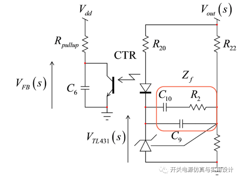
图1 设计者通常使用的传统II型补偿网络
If this association of passive elements is not wrong per se, it reflects a misconception of the circuit operation. In particular, the presence of a fast lane through resistor R20. By fast lane, I mean the fact that the LED current – which closes the feedback loop – does not only depend on the TL431 operation but also directly on Vout via R20. And that is the difficulty here: at high frequency, when C9 impedance is low, the TL431 ac current no longer depends on information brought by R22, the output voltage sensing network. So you expect a zero-current ac modulation in the LED imposed by the sensing network, nicely rolling off the gain. Unfortunately, as the TL431 cathode voltage is maintained in dc (like a programmable Zener diode), if Vout changes, the ac current in the LED undergoes modulation through R20: this is the fast lane effect, canceling the gain roll-off at high frequency as you would expect from an op amp-based type 2 circuit. 尽管这种无源器件的连接方式本身没错,但却反映了对电路运行机理的误解。尤其是电路中含电阻R20的快速通道。我的意思是,通过快速通道的LED电流闭环了反馈回路,本质上它不仅取决于TL431的工作状态,还直接取决于连接Vout的R20。这就是困难所在之处:尽管电容C9的阻抗在高频时变低,但TL431上的AC电流不再取决于分压网络中的R22。所以,你期望分压网络会强制LED中的AC电流信号为0,从而更好地衰减高频增益。不幸的是,TL431的阴极会保持在一个直流值(类似于一个可编程稳压管),如果Vout改变,通过R20的LED AC电流会变化调整(译者加:而不是经由分压网络中的R22):这就是快速通道效应,它抵消了你的预期——基于运放type 2型在高频处增益衰减的效果。Actually, when implementing the Figure 1 sketch, the designer expects to calculate elements values as with a type 2 compensator built around an op amp. However, because of the fast lane contribution, the transfer function totally differs as expressed by the simplified below low-Q definition: 事实上,当实现图1所示的意图时,设计人员希望像运算放大器构建type 2补偿器那样来计算元件值。然而,由于快速通道的存在,传递函数完全不同,正如下面简化的低Q值条件下的表达式:
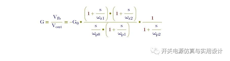

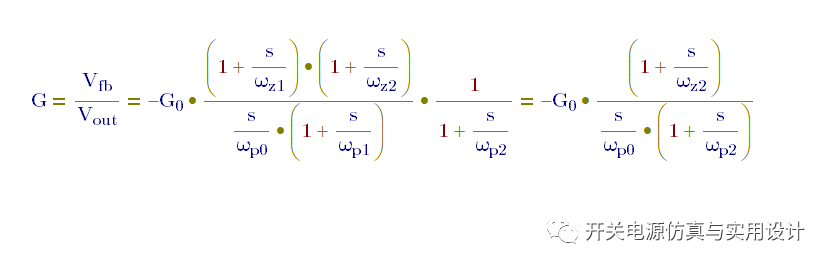
在这个表达式中,C2等于外加电容C6和光耦的寄生电容Copto的和,如果wz1和wp1靠的很近,那么它们彼此抵消,使得传递函数简化成另一种II型补偿的表达式:
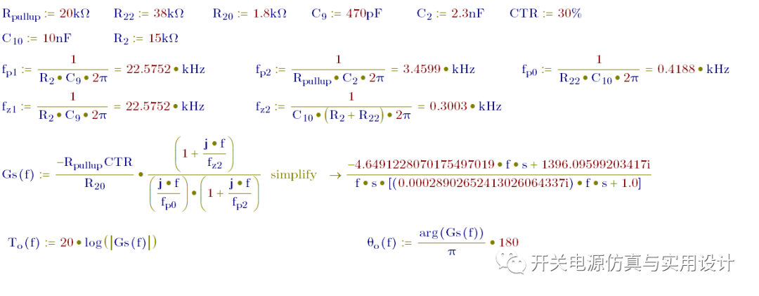
Rpullup = 20 kΩ, R22 = 38 kΩ, R20 = 1.8 kΩ, C9 = 470 pF, C2 = 2.3 nF, CTR = 30%, C10 = 10 nF and R2 = 15 kΩ.
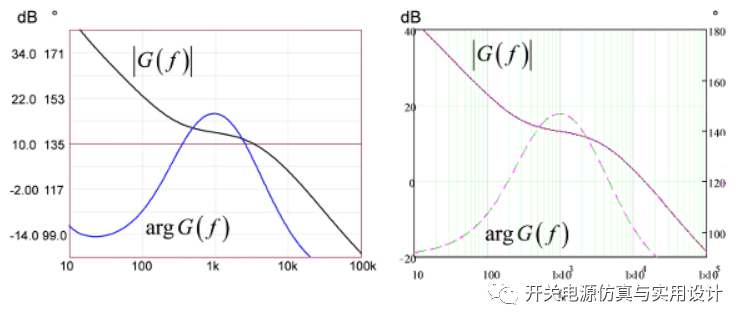
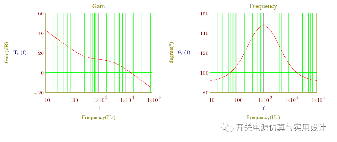
图 2 spice和mathcad获得的AC响应一致
With these values, the poles and zeros are located at:
根据这些值,极零点分布如下:
fz1 = 32.2 kHz, fz2 = 293 Hz, fp1 = 22.5 kHz and fp2 = 3.4 kHz
So yes, this is a type 2 response but you can obtain exactly the same response without the usage of the C10R2 network. A single capacitor connected between the TL431 cathode and the reference pin will not only introduce an origin pole, it will also produce a zero thanks to the fast lane action. The simpler schematic appears in Figure 3.
因此,这是一种可以不用C10、R2网络就可实现的type 2型补偿。得益于网络中的快通道,在TL431阴极和参考端放置单个电容,不仅引入了一个初始极点,还引入一个零点。其简化的原理图如下图3所示:
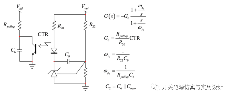
图3 正确使用TL431进行补偿只需一个电容
In conclusion, rather than compensating the TL431 as you would do with an op amp, it is best to capitalize on the fast lane presence and understand its role. When you do that, you realize that a single capacitor can do the job. This is the correct way to build a type 2 compensator with a TL431 and optocoupler. More details on how to design the compensator are given in Ref. 1.
总而言之,不要像使用运放那样使用TL431进行补偿,最好利用快速通道并理解其作用。当你Get到这一点的时候,你就会意识到单个电容足够完成补偿器的工作,这才是使用TL431和光耦构建type 2型补偿器的正确方法。关于如何设计补偿器的更多细节,请参考文献1。
Reference
-
Christophe Basso, “Designing Control Loops for Linear and Switching Power Supplies – A Tutorial Guide”, Artech House, Boston 2012, ISBN 978-1-60807-557-7
原文链接:
https://www.onsemi.com/blog/innovation-forum/single-capacitor-is-enough/
本文源自微信公众号:开关电源仿真与实用设计,不代表用户或本站观点,如有侵权,请联系nick.zong@aspencore.com 删除!
 0
0