PowerInt公司的InnoSwitch3-CE系列是集成了650V MOSFET,同步整流和FluxLink反馈的离线CV/CC QR反激开关集成电路,具有多种保护如线路过压和欠压保护,输出过压和过流限制,超温关断等,满负载效率高达94%,无负载功耗小于15mW,绝缘电压>4000 VAC,主要用在高达65W的高效反激电源,移动设备的大电流充电器和适配器,以及消费类电子如机顶盒(STB),网络,游戏和LED.本文介绍了InnoSwitch3-CE系列产品亮点,初级和次级控制器框图,典型应用电路,以及采用InnoSwitch3-CE, INN3168C-H101的65W电源参考设计DER535主要特性和指标,电路图,材料清单和PCB设计图.
The InnoSwitch™3-CE family of ICs dramatically simplifies the designand manufacture of flyback power converters, particularly thoserequiring high efficiency and/or compact size. The InnoSwitch3-CEfamily incorporates primary and secondary controllers and safety-ratedfeedback into a single IC.
InnoSwitch3-CE family devices incorporate multiple protection featuresincluding line over and under-voltage protection, output over-voltageand over-current limiting, and over-temperature shutdown. Devices areavailable that support the common combinations of latching andauto-restart behaviors required by applications such as chargers,adapters, consumer electronics and industrial systems. The devices areavailable with and without cable-drop compensation.
InnoSwitch3-CE系列产品亮点:
Highly Integrated, Compact Footprint
• Up to 94% efficiency across full load range
• Incorporates a multi-mode Quasi-Resonant (QR) / CCM flybackcontroller, 650 V MOSFET, secondary-side sensing and synchronousrectification driver
• Integrated FluxLink™, HIPOT-isolated, feedback link
• Exceptional CV/CC accuracy, independent of external components
• Adjustable accurate output current sense using external sense resistor
EcoSmart™ – Energy Efficient
• Less than 15 mW no-load including line sense
• Easily meets all global energy efficiency regulations
• Low heat dissipation
Advanced Protection / Safety Features
• Secondary MOSFET or diode short-circuit protection
• Open SR FET-gate detection
• Fast input line UV/OV protection
Optional Features
• Cable-drop compensation with multiple settings
• Variable output voltage, constant current profiles
• Auto-restart or latching fault response for output OVP/UVP
• Multiple output UV fault thresholds
• Latching or hysteretic primary over-temperature protection
Full Safety and Regulatory Compliance
• Reinforced isolation
• Isolation voltage >4000 VAC
• 100% production HIPOT testing
• UL1577 and TUV (EN60950) safety approved
• Excellent noise immunity enables designs that achieve class “A”performance criteria for EN61000-4 suite; EN61000-4-2, 4-3 (30V/m), 4-4, 4-5, 4-6, 4-8 (100 A/m) and 4-9 (1000 A/m) and FordFMC1278 (RI-115)
Green Package
• Halogen free and RoHS compliant
InnoSwitch3-CE系列应用:
• High efficiency flyback designs up to 65 W
• High current charger and adaptors for mobile devices
• Consumer electronics − set-top boxes, networking, gaming, LED
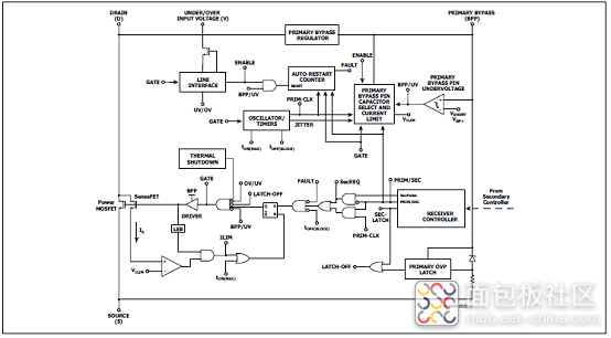
图1.InnoSwitch3-CE系列初级控制器框图
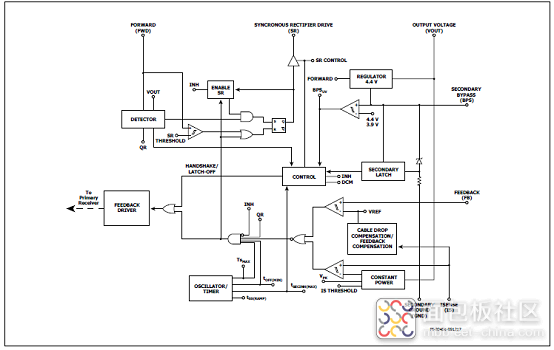
图2.InnoSwitch3-CE系列次级控制器框图
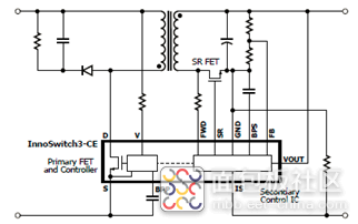
图3.InnoSwitch3-CE系列典型应用电路图
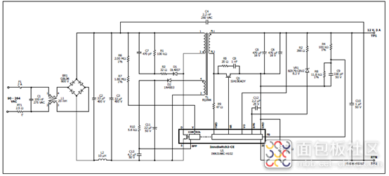
图4.InnoSwitch3-CE系列应用电路:12V/3A充电器/适配器
采用InnoSwitch3-CE, INN3168C-H101的65W电源参考设计DER535
This document is an engineering report describing a 19 V, 3.4 A power supply utilizingINN3168C from the InnoSwitch3-CH family of ICs.
This design shows the high power density and efficiency that is possible due to the high level of integration while still providing exceptional performance.
The document contains the power supply specification, schematic, bill of materials,transformer documentation, printed circuit layout, and performance data.
65W电源参考设计DER535主要特性:
Built in synchronous rectification for >90% efficiency without NTC at nominal AC input
All the benefits of secondary side control with the simplicity of primary side regulation
Insensitive to transformer variation
Extremely fast transient response independent of load timing
Secondary sensed output overvoltage protection (OVP) for accurate fault protection
Accurate thermal protection with hysteretic shutdown
Input voltage monitor with accurate brown-in/brown-out and overvoltage protection
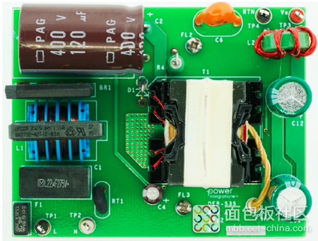
图5. 65W电源参考设计DER535外形图(正面)
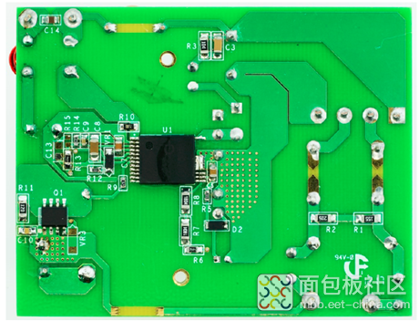
图6. 65W电源参考设计DER535外形图(背面)
65W电源参考设计DER535主要指标:
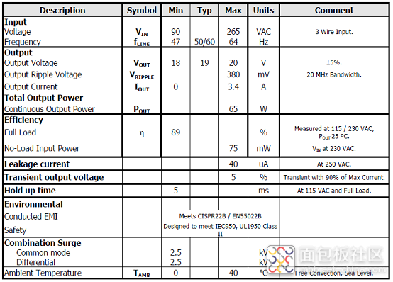
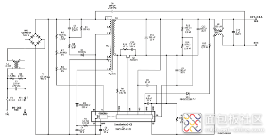
图7. 65W电源参考设计DER535电路图
65W电源参考设计DER53材料清单:
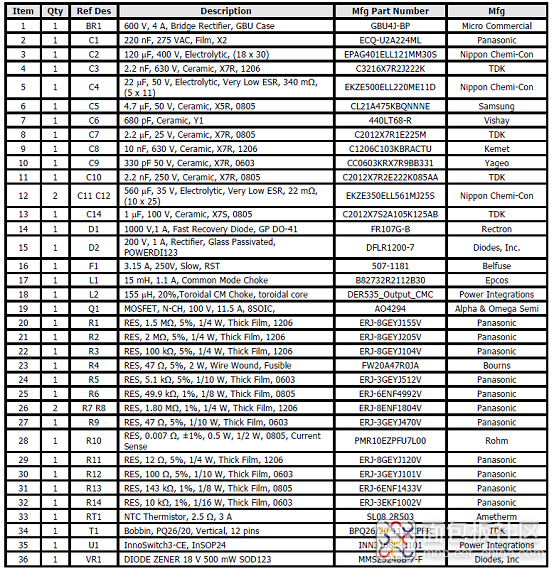
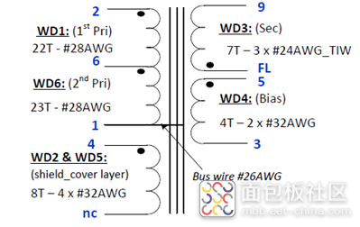
图8. 65W电源参考设计DER535变压器电路图
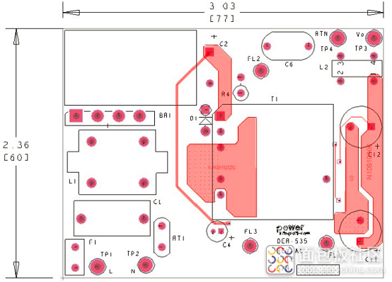
图9. 65W电源参考设计DER535 PCB设计图(正面)
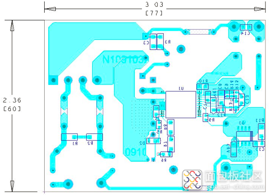
图10. 65W电源参考设计DER535 PCB设计图(背面)
The InnoSwitch™3-CE family of ICs dramatically simplifies the designand manufacture of flyback power converters, particularly thoserequiring high efficiency and/or compact size. The InnoSwitch3-CEfamily incorporates primary and secondary controllers and safety-ratedfeedback into a single IC.
InnoSwitch3-CE family devices incorporate multiple protection featuresincluding line over and under-voltage protection, output over-voltageand over-current limiting, and over-temperature shutdown. Devices areavailable that support the common combinations of latching andauto-restart behaviors required by applications such as chargers,adapters, consumer electronics and industrial systems. The devices areavailable with and without cable-drop compensation.
InnoSwitch3-CE系列产品亮点:
Highly Integrated, Compact Footprint
• Up to 94% efficiency across full load range
• Incorporates a multi-mode Quasi-Resonant (QR) / CCM flybackcontroller, 650 V MOSFET, secondary-side sensing and synchronousrectification driver
• Integrated FluxLink™, HIPOT-isolated, feedback link
• Exceptional CV/CC accuracy, independent of external components
• Adjustable accurate output current sense using external sense resistor
EcoSmart™ – Energy Efficient
• Less than 15 mW no-load including line sense
• Easily meets all global energy efficiency regulations
• Low heat dissipation
Advanced Protection / Safety Features
• Secondary MOSFET or diode short-circuit protection
• Open SR FET-gate detection
• Fast input line UV/OV protection
Optional Features
• Cable-drop compensation with multiple settings
• Variable output voltage, constant current profiles
• Auto-restart or latching fault response for output OVP/UVP
• Multiple output UV fault thresholds
• Latching or hysteretic primary over-temperature protection
Full Safety and Regulatory Compliance
• Reinforced isolation
• Isolation voltage >4000 VAC
• 100% production HIPOT testing
• UL1577 and TUV (EN60950) safety approved
• Excellent noise immunity enables designs that achieve class “A”performance criteria for EN61000-4 suite; EN61000-4-2, 4-3 (30V/m), 4-4, 4-5, 4-6, 4-8 (100 A/m) and 4-9 (1000 A/m) and FordFMC1278 (RI-115)
Green Package
• Halogen free and RoHS compliant
InnoSwitch3-CE系列应用:
• High efficiency flyback designs up to 65 W
• High current charger and adaptors for mobile devices
• Consumer electronics − set-top boxes, networking, gaming, LED

图1.InnoSwitch3-CE系列初级控制器框图

图2.InnoSwitch3-CE系列次级控制器框图

图3.InnoSwitch3-CE系列典型应用电路图

图4.InnoSwitch3-CE系列应用电路:12V/3A充电器/适配器
采用InnoSwitch3-CE, INN3168C-H101的65W电源参考设计DER535
This document is an engineering report describing a 19 V, 3.4 A power supply utilizingINN3168C from the InnoSwitch3-CH family of ICs.
This design shows the high power density and efficiency that is possible due to the high level of integration while still providing exceptional performance.
The document contains the power supply specification, schematic, bill of materials,transformer documentation, printed circuit layout, and performance data.
65W电源参考设计DER535主要特性:
Built in synchronous rectification for >90% efficiency without NTC at nominal AC input
All the benefits of secondary side control with the simplicity of primary side regulation
Insensitive to transformer variation
Extremely fast transient response independent of load timing
Secondary sensed output overvoltage protection (OVP) for accurate fault protection
Accurate thermal protection with hysteretic shutdown
Input voltage monitor with accurate brown-in/brown-out and overvoltage protection

图5. 65W电源参考设计DER535外形图(正面)

图6. 65W电源参考设计DER535外形图(背面)
65W电源参考设计DER535主要指标:


图7. 65W电源参考设计DER535电路图
65W电源参考设计DER53材料清单:


图8. 65W电源参考设计DER535变压器电路图

图9. 65W电源参考设计DER535 PCB设计图(正面)

图10. 65W电源参考设计DER535 PCB设计图(背面)


 /4
/4 
