安规,EMI,PCB布局基本知识回顾!
很难得的接地气的资料!
Refreshing Basics on Safety EMI PCB Layout
by
Dr. Supratim Basu, Bose Research Pvt Ltd.
Prof. Tore. M. Undeland, NTNU
Controlling EMI issues in Power Electronics Designs
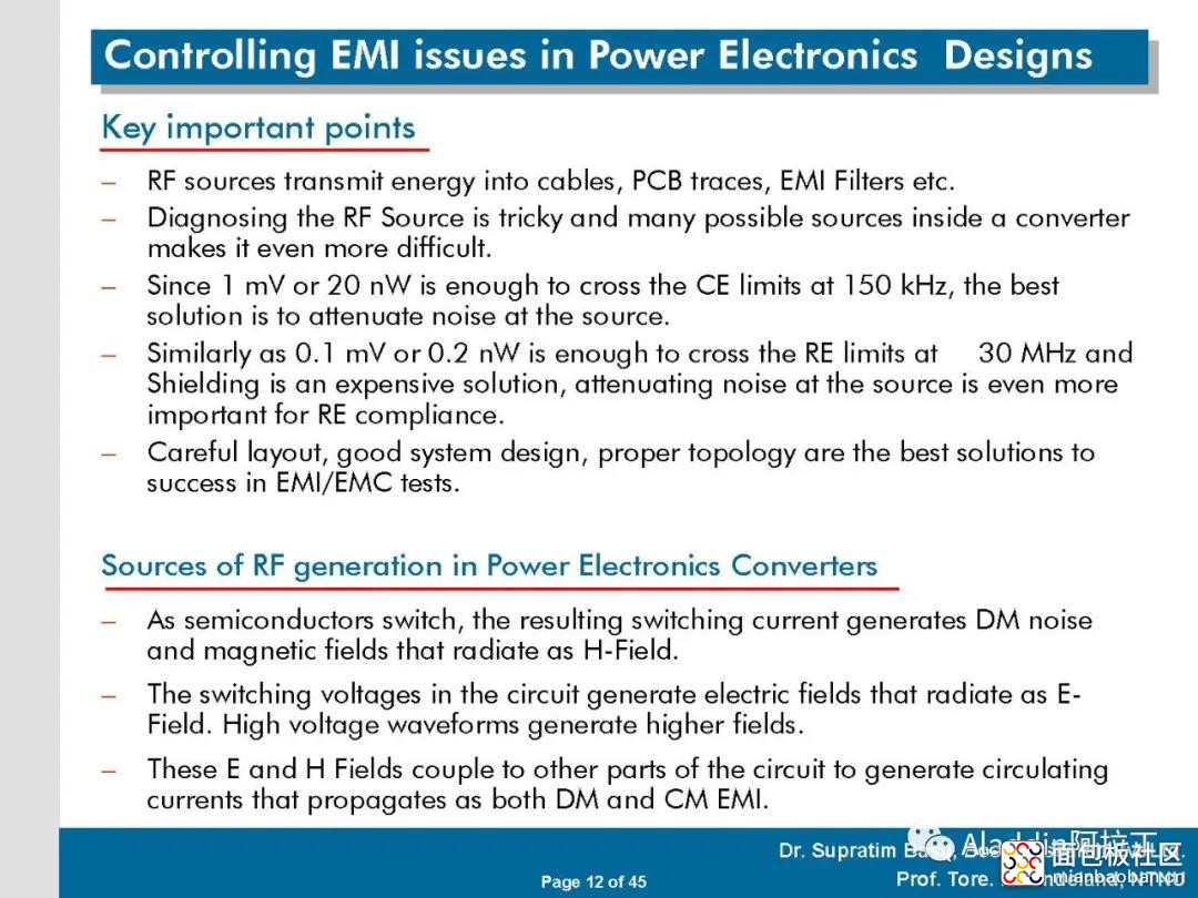
- RF sources transmit energy into cables, PCB traces, EMI Filters etc.
- Diagnosing the RF Source is tricky and many possible sources inside a converter makes it even more difficult.
- Since 1 mV or 20 nW is enough to cross the CE limits at 150 kHz, the best solution is to attenuate noise at the source.
- Similarly as 0.1 mV or 0.2 nW is enough to cross the RE limits at 30 MHz and Shielding is an expensive solution, attenuating noise at the source is even more important for RE compliance.
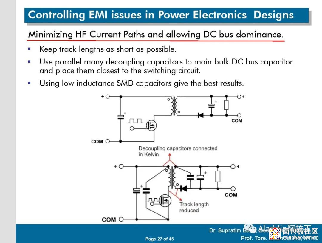
- Careful layout, good system design, proper topology are the best solutions to success in EMI/EMC tests.
Sources of RF generation in Power Electronics Converters
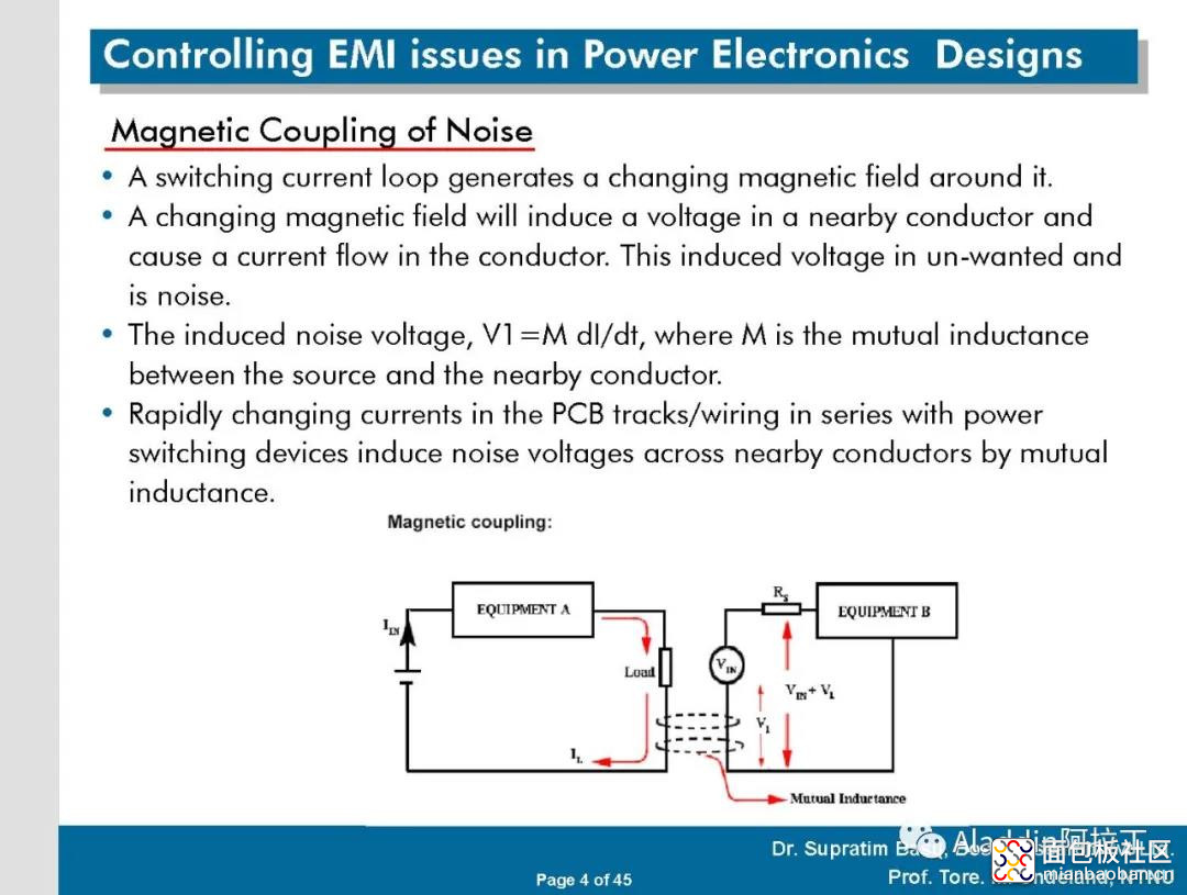
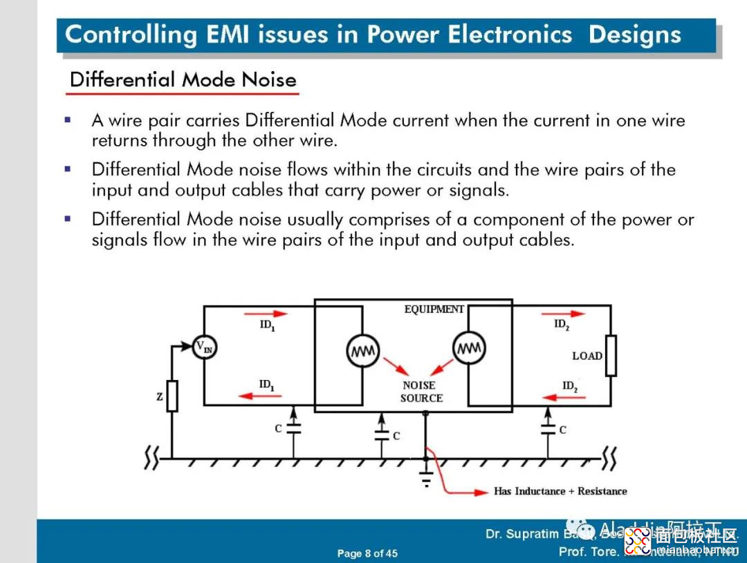
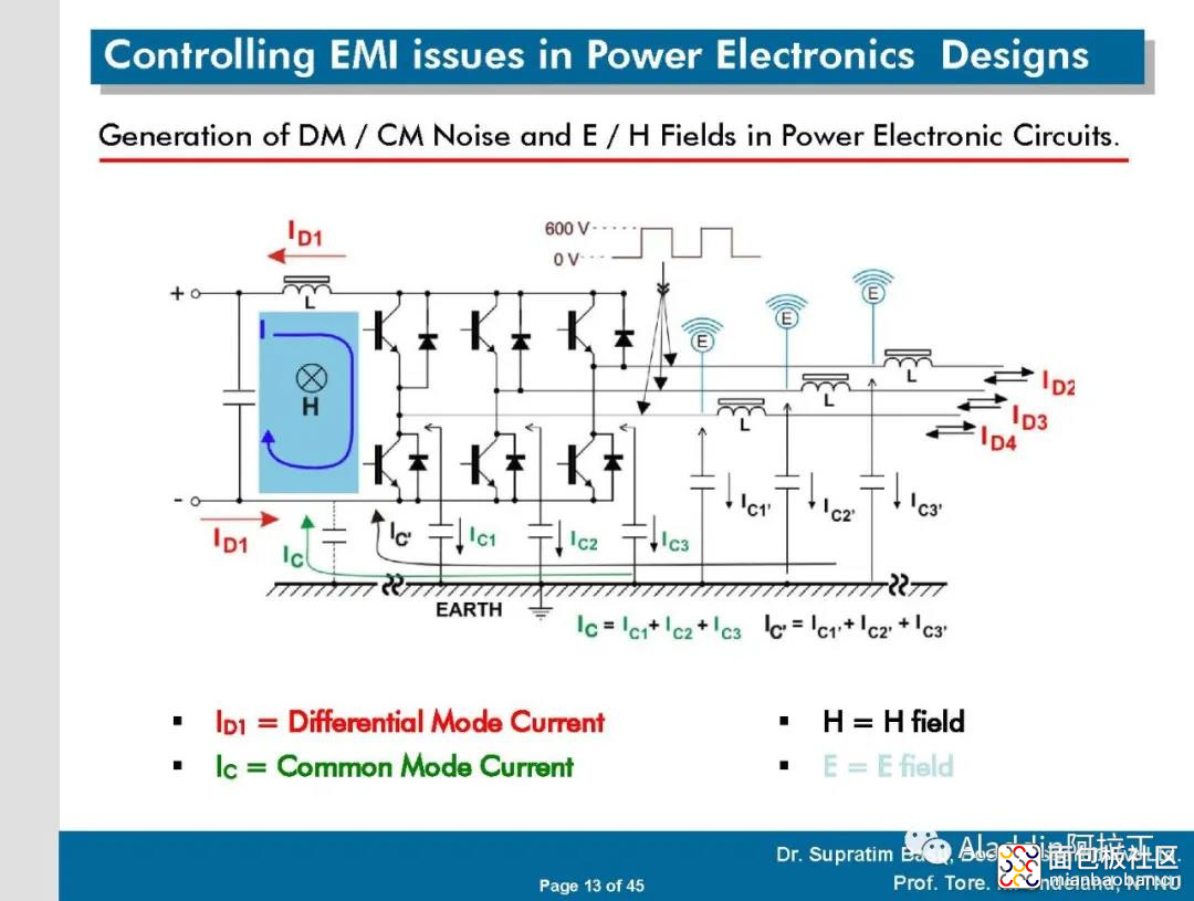
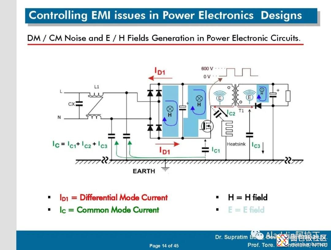
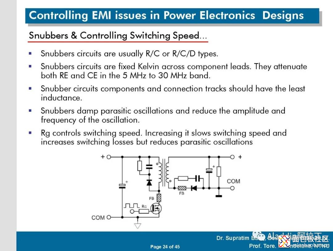
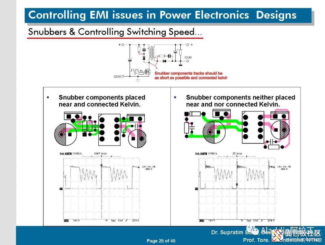
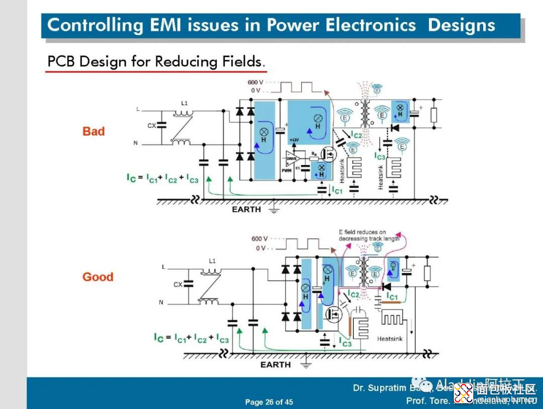
- As semiconductors switch, the resulting switching current generates DM noise and magnetic fields that radiate as H-Field.
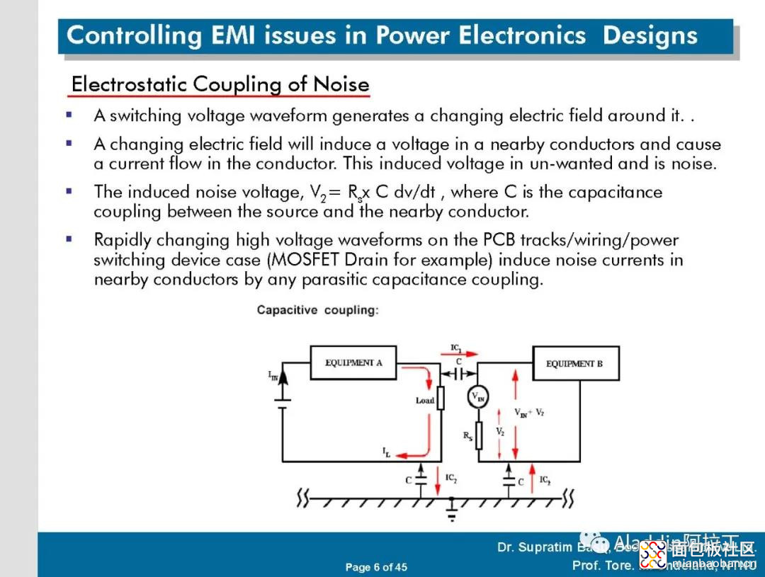
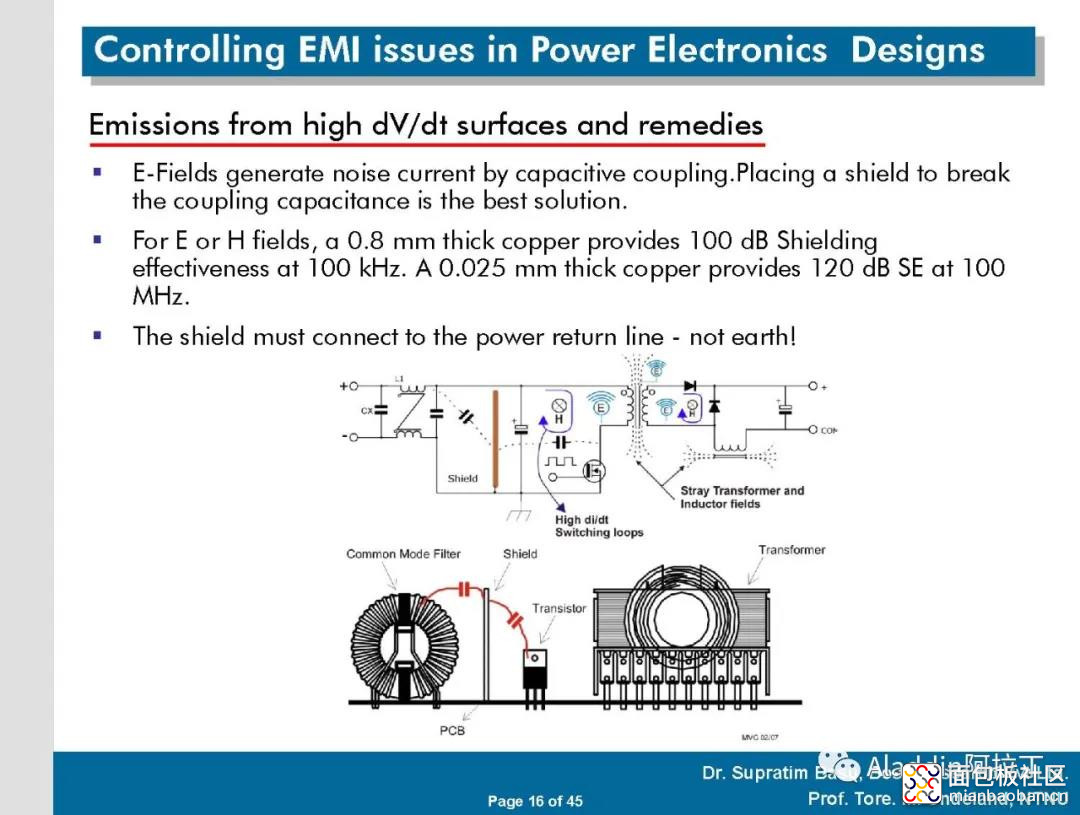
- The switching voltages in the circuit generate electric fields that radiate as E-Field. High voltage waveforms generate higher fields.
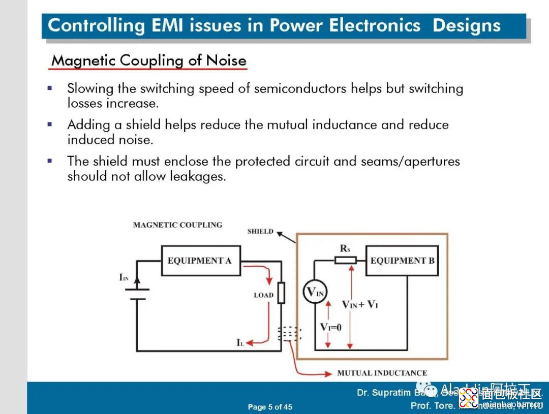
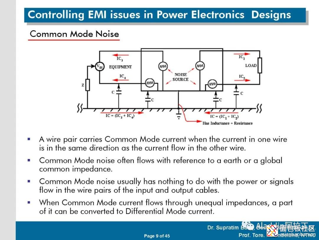
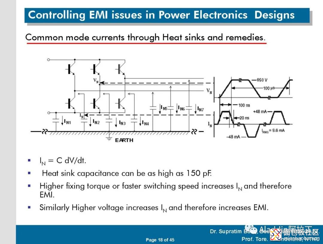
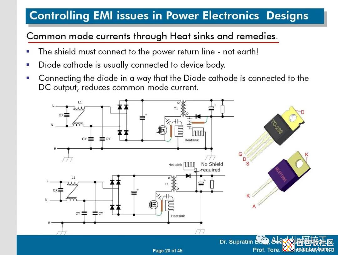
- These E and H Fields couple to other parts of the circuit to generate circulating currents that propagates as both DM and CM EMI.
感谢文老师的允许转载,
感谢博士 Supratim Basu。
来源微信公众号:Aladdin阿拉丁
转载链接:https://mp.weixin.qq.com/s/ZCkfNcoWVuc6h0LjKWDuTQ


 /5
/5 


